Megatrend · Semiconductors
The software that designs every chip in the world — and America holds three of the keys
Before a single chip is ever made in a fab, it has to be 'designed.' And a modern chip with tens of billions of transistors can no longer be drawn by hand — it takes a special kind of software (EDA) plus 'ready-made circuit blocks' (IP) you buy and assemble. The striking part: both are concentrated in the hands of just a few companies, making this the quietest yet most powerful bottleneck in the chip world — and a weapon in the US–China tech war.
01What EDA and IP are
We often say a Foundry is the fab that makes chips, and an EUV machine is the equipment that prints the circuits. But here's a question people skip: before you 'make' a chip, who actually 'designs' it? And what does the blueprint sent to the fab even look like?
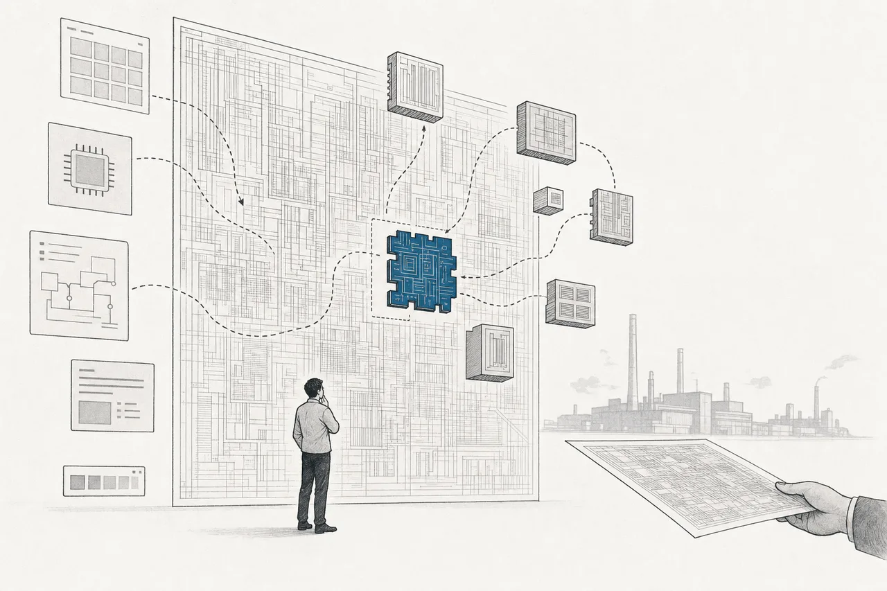
The answer is that modern chips can no longer be designed by hand. A single phone or AI chip has tens to hundreds of billions of transistors. Picture city planning with hundreds of billions of roads that all have to avoid collisions, never lose power, and flow as fast as possible — impossible to draw by hand. That's where this node comes in. It's the 'tools and raw materials for designing chips,' made of two big parts:
- EDA (Electronic Design Automation): software that helps people design, simulate, and verify chips — think 'the AutoCAD of the chip world,' but far smarter. It lays out billions of transistors, draws the connections, simulates whether the circuit actually works, and catches bugs before the (enormously expensive) real manufacturing
- Semiconductor IP (chip IP): 'ready-made circuit blocks' already designed and licensed out — instead of designing a CPU, a memory controller, or a USB port from scratch (which takes years), a company buys these 'blocks' and snaps them together like Lego
EDA = the suite of chip-design software (synthesis, simulation, place-and-route, verification) · IP core = a ready-made circuit design licensed for use (e.g. Arm's CPU, a PCIe controller, a memory interface) · RTL (Register-Transfer Level) = the language engineers use to 'describe' a circuit's behavior (e.g. Verilog/VHDL), much like program code, before EDA translates it into a real transistor layout.
On our megatrend map, this node sits under Semiconductors and is the 'furthest upstream' layer (platform) — even before wafer-fab equipment or the foundry. Because every chip in the world, whether made at TSMC, Samsung, or Intel, has to pass through EDA tools and is usually assembled from IP first. It's the 'common language' the whole industry speaks.
02Why it matters to the world
The reason this small node holds enormous power is that it's a bottleneck. Almost every advanced chip on Earth — from NVIDIA's AI chips to the iPhone's chip to the chips in your car — is designed with software from just 3 companies: Synopsys and Cadence (US), and Siemens EDA (Germany / formerly America's Mentor Graphics).
This concentration is nearly a monopoly: Synopsys holds ~31% of the market, Cadence ~30%, Siemens ~13% — together ~74% of the entire global EDA market. And if you count only the tools used to design the most cutting-edge chips, the three together control over 90% of the revenue — there's almost no way to design an advanced chip without paying these three.
This isn't the biggest market in the chip world — total value is around $15–19 billion in 2025 (many times smaller than the foundry market). But its 'power' far outweighs its size, because it sits furthest upstream. Every $1 paid to EDA unlocks hundreds of dollars of chip manufacturing downstream. And crucially, it grows faster than the chip industry's own R&D spending — EDA grows about 13% a year while semiconductor R&D budgets grow only ~7%, because the more complex chips get, the more they lean on software.
03How it works
Follow a single chip from 'idea' to 'blueprint sent to the fab' and you'll see EDA and IP woven into every step:
The heart of what makes this hard is 'verification'. Imagine getting even one spot wrong among tens of billions of transistors and only 'finding out after it's manufactured' — the damage runs to hundreds of millions of dollars, because you have to remake the whole run. So EDA isn't just a drawing tool but a 'simulator and bug-catcher' that has to prove a chip will work correctly before any real money is spent.
A number to make it concrete: designing a single 2-nanometer chip costs about $725 million — and the biggest chunk isn't the fab, it's the software and verification — roughly $314 million for software/firmware and another ~$154 million for verification, together the largest share of the bill. That's why EDA is a high-margin business.
04The 'tollbooth' model of Arm and RISC-V
The other half of this node is chip IP, and no one tells this story better than Arm, the British company (under SoftBank) that designs the 'CPU architecture' found in nearly every phone on Earth. The striking part: Arm doesn't make a single chip, and doesn't even sell chips — it just designs, then collects a small 'toll (royalty)' on every chip that uses its design.
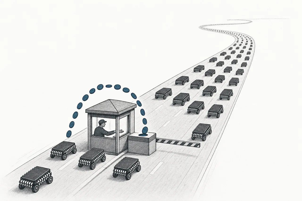
This model has two layers of revenue: (1) a licensing fee — an upfront payment for the right to use the design — and (2) a royalty fee — paid per chip sold. The second layer is the charm: of about $4.67 billion in revenue (trailing 12 months), royalties make up ~$2.55 billion, nearly 55% — a stream that flows in every year from chips sold in the past. And the more Arm pushes its newer architecture (v9, which charges higher royalties), the more revenue per chip grows — in 2025, v9 royalties overtook the older v7 for the first time.
The market values this model very highly. When Arm went public (IPO) in September 2023, it was worth around $52 billion. But once the AI wave hit (NVIDIA's Grace CPU also uses Arm), its value surged to about $150 billion in 2026 — priced like a growth stock, even though at its core it's a 'tollbooth' business.
ISA (Instruction Set Architecture) = the basic 'command language' a chip understands — Arm and x86 (Intel/AMD) are ISAs you pay to use · RISC-V is an open and free (open-source) ISA anyone can use to design chips without paying royalties — like 'the Linux of the chip world.' It's gaining momentum in IoT devices, cars, and Edge AI, and is being pushed by China and India as a 'national standard' to escape reliance on Western technology.

RISC-V is growing alarmingly fast: by the end of 2025, there were about 20 billion RISC-V cores worldwide, holding roughly 25% of the chip market (faster than many expected). In December 2025, Qualcomm even acquired Ventana, a high-end RISC-V CPU company, to gain leverage in its licensing fight with Arm — a signal that the 'open' model is seriously pressuring the 'tollbooth' one.
05How it connects in the ecosystem
This node is the 'upstream of the upstream.' Everything in the chip world starts here:
- Comes before Foundry and Wafer-Fab Equipment: if a foundry is the 'construction site,' this node is the 'architect and the blueprints.' The blueprint (GDSII) that EDA produces is exactly what gets handed to TSMC to make — no design, nothing to build. And EDA and the foundry have to work tightly together, because the tools must know each node's manufacturing 'design rules.'
- Feeds AI directly — and AI feeds back: the hottest two-way relationship. On one side, every AI chip (including NVIDIA's GPUs) is designed with EDA. On the other, AI is coming in to help design chips itself — new EDA tools use AI to explore millions of possible layouts to find the best one.
- Opens the way for electric vehicles, robots, and Quantum: every trend that needs specialized chips has to design them first — the more the world wants 'custom' silicon, the more demand grows for EDA and IP.
- Acts as a 'switch' in the supply chain and geopolitics game: because EDA is concentrated in the hands of the US and its allies, it's the point where a government can 'flip a switch' to control a rival country's chip-design ability (more on that in the next chapter).
06Where it stands now
Two big stories define this moment: AI entering chip design and EDA becoming a weapon in the trade war.
The first — 'AI designing chips' is becoming real. Cadence launched Cerebrus AI Studio, which uses agentic AI to help with layout, claiming it can improve a chip (PPA — power/performance/area) by up to 20% and speed up design time 5–10x; chips using this tool have already taped out over 1,000 times. On Synopsys's side, DSO.ai and Synopsys.ai Copilot claim to raise productivity more than 3x and improve output quality by up to 20%.
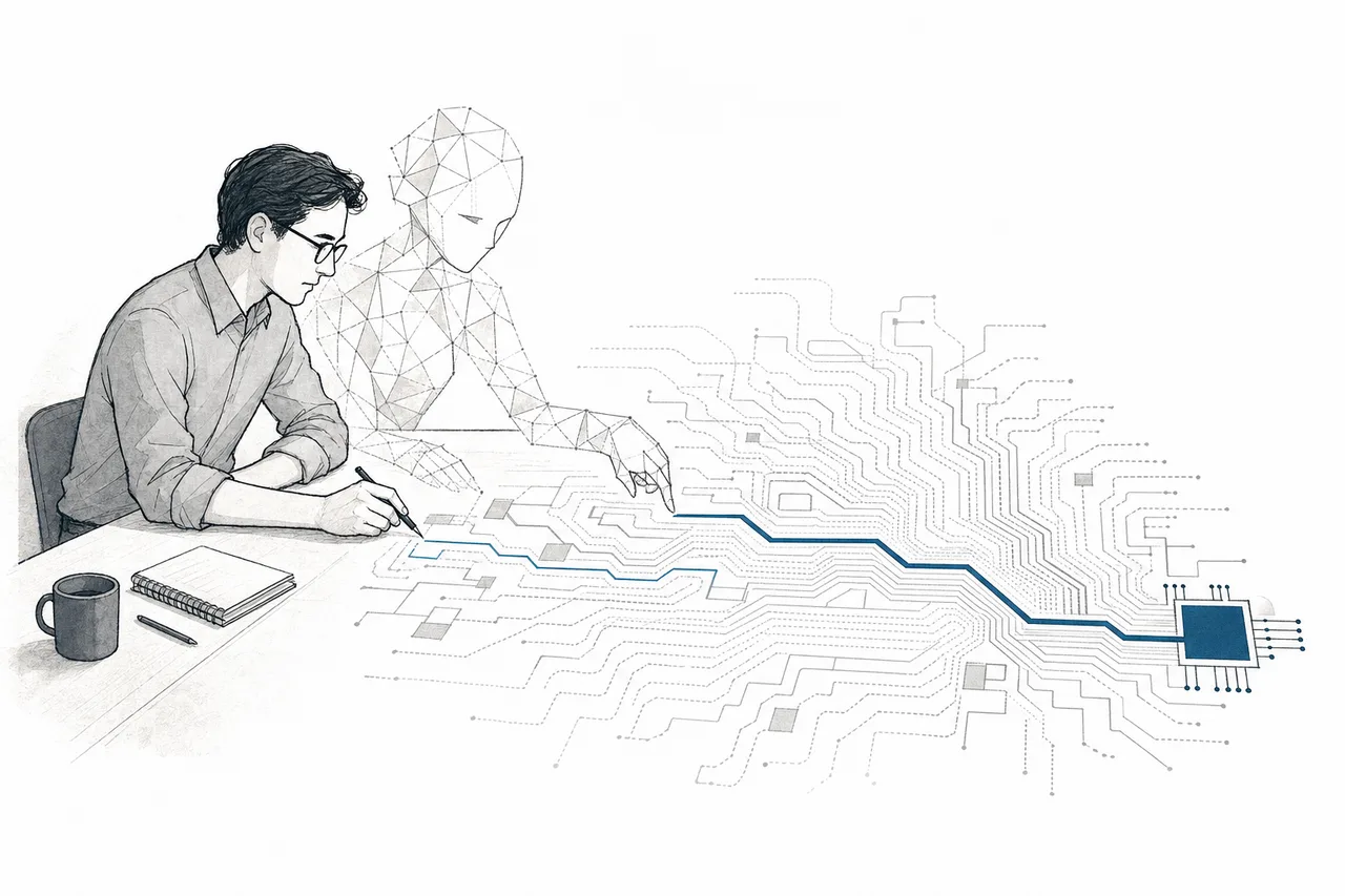
This is 'AI eating its own tail' in the good sense — AI chips that get harder and harder to design need AI to help design them, making EDA both a user and a driver of the AI era at once. It's a key reason Synopsys/Cadence stocks command such a high premium.
The second — EDA became a center-board piece in the US–China chip fight. In May 2025, the US Commerce Department (BIS) ordered Synopsys, Cadence, and Siemens EDA to obtain a license before selling to China, citing the risk of military use — effectively 'cutting off the water' to China's advanced chip-design ability overnight.
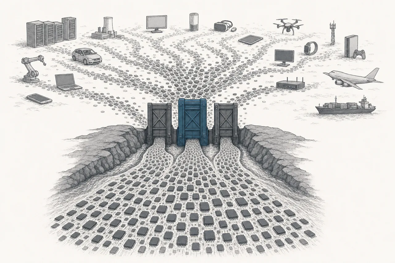
The impact showed up in dollars immediately — China is a big market for both: Synopsys earned nearly $1 billion from China in fiscal 2024 (~16% of total revenue), and Cadence about $550 million (~12%), with the Big-3 together holding ~78–80% of China's EDA market. Both stocks dropped right after the news — but the plot twisted: by early July 2025, the US lifted the restriction (partly from trade negotiations), and the stocks bounced back. The whole episode lasted just ~5 weeks, but it drove home to the world that EDA is a 'tap' that really can be turned on and off.
07The road ahead
The first direction: AI will absorb EDA into itself. From a tool that 'engineers command,' it's becoming a 'co-designing assistant' — and the far goal is agentic EDA that takes a high-level request ('give me the lowest-power chip for this job') and designs most of it on its own. If it really works, it would slash design time and cost enormously and let Synopsys/Cadence sell 'outcomes' rather than just 'software licenses.'
The second direction: custom silicon booms. As big companies (Google, Amazon, Tesla, Microsoft) turn to designing their own chips instead of buying off-the-shelf, demand for EDA tools and IP blocks grows with it — every new 'custom' chip is a new customer for this node.
The third direction: RISC-V and the politics of 'ownership'. The more China and other countries fear being 'cut off' the way they saw in 2025, the more they flee to open and free options like RISC-V and rush to build their own EDA. This may slowly erode the monopoly over the long run — but slowly, because the Big-3's ecosystem (tools, libraries, skilled engineers) is too deep to copy in a few years.
08Challenges & risks
The node that looks safest (high margins, monopolistic, recurring revenue) has its own cracks too.
The first risk is dependence on China and policy volatility. The 2025 drama showed that 12–16% of revenue from China can 'vanish overnight' with a single letter. And even though that round was reversed in 5 weeks, this risk circles back every time US–China tensions flare — a risk that lives off the balance sheet, but on the negotiating tables of heads of state.
The second risk is RISC-V and open-source EDA. As long as Arm charges royalties and the Big-3 charge high software fees, the world has an incentive to seek free alternatives. Qualcomm buying Ventana, and China/India pushing RISC-V as a national standard, are signs that the 'licensing wall' is being challenged — and if one day the open ecosystem ripens enough, the tollbooth model could get squeezed.
The third risk is concentration of customers and technology. This node's big revenue is tied to advanced chips, which are tied to a few customers (and to the AI boom). If AI investment slows, or chip architectures change how design is done in a major way, demand for the old kind of tools could stall. And on the IP side, Arm's lesson is that 'a leader who misses a single architecture can lose the throne.'
In short: before a single chip lands in your phone, your car, or an AI data center, it's first 'written' with software and circuit blocks from just a few players. This quietest, most invisible node is where an entire country's chip-design ability is decided — and it's why 'chip-design software' has become a phrase on the world's trade-negotiation tables, not just in the engineers' room anymore.