Megatrend · Semiconductors
The machines that make chips: the industry's deepest moat
Everyone talks about NVIDIA and TSMC. But hidden behind them is a quieter, far more monopolized industry — the handful of companies that build the 'machines used to make chips.' One of them is a Dutch firm that is the only company on Earth able to make a machine costing ~$380 million each — a bottleneck that the US and China are fighting over. This lesson walks through why the 'equipment layer' is where the real power of the AI era concentrates.
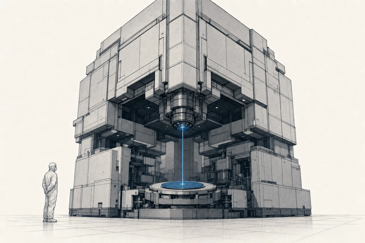
01What it is (three families of equipment)
Picture a round disc of silicon about the size of a dinner plate (it's called a 'wafer'). You have to build transistors — tiny electrical switches — onto it, tens of billions of them, each one smaller than a virus, and every one has to work. This isn't a job you do by hand. It takes the most precise machines humanity has ever built — and this node is the story of those machines.
On the megatrend map, Wafer-Fab Equipment is a sub-branch under Semiconductors. Its definition is short but powerful: 'the tools that print, deposit, etch and inspect the wafer — the layer with the deepest moat.' Making a single chip means cycling through these steps hundreds of times, and each step needs a different family of machine. This node splits into three sub-categories by function:
- Lithography (printing): the machine that 'shines' the circuit pattern onto the wafer, like a photo printer — except the pattern it prints is just a few nanometers wide. This is the category ASML monopolizes at the leading edge ·
- Deposition & Etch (coating & carving): the machines that 'coat' ultra-thin layers of material on (deposition) then 'carve' away what isn't wanted (etch) — like sculpting a shape by adding and shaving layer by layer. The leaders are Applied Materials, Lam Research and Tokyo Electron ·
- Process Control (inspection): the machines that 'look closely' to find defects and measure precision at every step — because a single tiny defect ruins the whole chip. This category KLA dominates by a wide margin .
Fab = the plant that makes chips (fabrication plant) · WFE = all the machines inside it that turn blank wafers into chips. When investors talk about 'TSMC's capex,' most of that money is going to buy WFE — simply put, WFE is the 'picks and shovels' every chip foundry has to buy, whether it's TSMC, Samsung, Intel or SMIC.
Investors like to call this business the 'picks and shovels' play — in the gold rush, the miners struck it rich or went bust, but the people selling 'picks and shovels' got rich every time. Because no matter who wins the AI-chip race, everyone ends up buying their machines from this same node.
02Why it's the layer with the deepest moat
The first reason is size and growth. The global WFE market in 2025 sits at around $125 billion, and counting all chipmaking tools, SEMI expects a new record of ~$139 billion in 2026, driven by one clear force — investment in AI chips, in both leading-edge logic and HBM memory, with no sign of slowing.
The second reason — and the heart of it — is intense concentration. Almost every sub-category in this node is held by 1–3 companies, and some leading-edge machines have just one maker in the world. Together the five giants — ASML, Applied Materials, Lam Research, Tokyo Electron, KLA — hold about 60–66% of the entire global chipmaking-equipment market, and the more advanced the tool, the more concentrated it gets.
Why is the moat this deep? Because building these machines is decades of accumulated know-how; each one has hundreds of thousands of parts from suppliers worldwide, and demands a precision no newcomer can copy in time. This is why China — pouring vast sums into self-sufficiency — still can't build the most advanced machines itself and must rely on Western and Japanese ones. Being 'cut off' from these machines has become one of the most powerful geopolitical weapons of the era.
03Lithography — printing patterns with light
If you had to pick the single 'most important and most monopolized' category in this node, the answer is lithography — 'printing the circuit pattern' with light. The principle is like developing film photos of old: you shine light through a 'master' (called a mask) onto a wafer coated with a light-sensitive material, and the light that lands 'prints' the circuit pattern. The catch: the smaller the pattern you want, the shorter the wavelength of light you need.
This is where EUV (Extreme Ultraviolet) comes from — light with a wavelength of just 13.5 nanometers (about 14x shorter than what older machines use) that makes 5nm, 3nm and 2nm patterns possible. And the way ASML creates this light is almost unbelievable:
About 50,000 droplets of tin per second are fired into a vacuum chamber, then hit twice by a high-power CO2 laser until the tin vaporizes into plasma reaching ~220,000°C (about 40x hotter than the sun's surface), emitting EUV light. And because nearly every material absorbs EUV light, ordinary glass lenses can't be used — ASML relies on multilayer mirrors from Germany's Zeiss, so smooth that 'if you scaled one up to the size of Germany, the largest bump would be no more than a few millimeters.'
DUV (Deep Ultraviolet) = the older machine, using longer-wavelength light (193nm) to make chips at 7nm and above — Japan's Canon/Nikon still compete in this market · EUV = 13.5nm light making 5/3/2nm, with ASML the only maker · High-NA EUV = a new EUV with a wider 'aperture' (NA 0.55) that makes even smaller patterns, at ~$380 million per machine — one machine costs about as much as two passenger jets.
This is why EUV is the 'bottleneck inside the bottleneck' — China has been barred from buying EUV since 2019 (the result of US pressure on the Dutch government), making advanced chips hard to produce. It has to loop older DUV machines many times instead, which is slow and low-yield. Controlling this one machine has become one of the most important keys in the great-power race for chip supremacy.
04Deposition, Etch & Process Control
Lithography grabs the headlines thanks to ASML, but the truth is litho is only about a quarter of the total equipment value. The other three-quarters is deposition & etch and process control — categories outsiders have barely heard of, yet where the biggest money flows, and the arena US and Japanese companies dominate.
Deposition (coating film) is layering material a few atoms thick onto the wafer — some techniques (ALD) deposit one atomic layer at a time. Etch (carving) is precisely removing the parts you don't want. Modern chips with complex 3D structures (like GAA transistors and NAND stacked over 200 layers) make deposition/etch steps multiply enormously — pushing these two machine families into quiet but powerful growth engines.
The etch arena is heavily concentrated — the top three (Lam Research, Tokyo Electron, Applied Materials) together hold about 90% of the market, with Lam Research controlling over 50% of dry etch, and Applied Materials holding the broadest portfolio — it makes almost every machine except litho.
The third category — Process Control (metrology & inspection) — is the 'quality checkpoint' embedded in every step. When transistors are nanometers across, a single defect invisible to the eye ruins the whole chip. The machines here 'hunt for defects' and 'measure whether each layer landed in the right position' (overlay) — and the more complex the chip, the more frequently it has to be checked.
Here KLA dominates more decisively than anyone in this node — about 56% of the whole process-control market, and over 85% in optical wafer inspection. It's a classic case of a business that's 'not the biggest, but the most monopolized' — and because AI chips demand the highest yield, demand for inspection machines grows right alongside.
05How it connects in the ecosystem
This node sits at the very 'top of the stream' of the chip supply chain — everything downstream has to pass through its machines first:
- Foundry and memory makers buy its machines: the main customers are TSMC, Samsung, Intel, SK Hynix, Micron, SMIC — most of their enormous capex is spent buying machines from this node. So the chip industry's 'up-and-down cycle' is also the cycle of the equipment companies.
- Feeds the AI wave indirectly but deeply: every NVIDIA AI chip and every stick of HBM is built on these machines. The more the world invests in AI, the more foundries order machines — this is the real 'picks and shovels' of the AI era.
- Opens the way for Cloud, electric vehicles, robots and Quantum: every trend that needs leading-edge chips leans on this node's machines, directly and indirectly.
- Depends on critical raw materials: each machine has hundreds of thousands of parts from suppliers worldwide, from special lenses and mirrors to rare metals, making it sensitive to any strain in the global supply chain.
06Where it stands now
2025–2026 is the peak period for this node — AI-chip demand has pushed machine orders to new records. ASML closed 2025 with €32.7 billion in revenue (up 15%), and more importantly a backlog of €38.8 billion — reflecting advance orders stretching years out. The company is targeting €44–60 billion in revenue by 2030, on the High-NA machine ramp and a second wave from HBM memory.
The hottest story of this period is the arrival of the High-NA EUV machine — the new model at ~$380 million each. ASML shipped the first one to Intel in late 2023 and is rolling them out to TSMC and Samsung to pave the way to 1.4nm chips and smaller. It's a bet on 'whoever gets the most advanced machine first' = 'whoever can build the next generation of AI chips first.'
The other side is the tech war with China, growing more intense. In Q4 2025, about 36% of ASML's machine sales still went to China (mostly the DUV models it can still sell). But by Q1 2026 the figure plunged to ~19% after tighter controls — a sign the door is slowly closing.
China is responding by racing to build its own machines. NAURA, China's largest equipment maker, grew revenue ~30% in the first half of 2025 and has begun testing etch machines on SMIC's 7nm production line, while SMEE tries to catch up in litho (but is still stuck at 28nm DUV). Some analysts think China-made machines could hold 50–60% of the machines in Chinese fabs by 2030 — but mostly older nodes, not the leading edge.
07The road ahead
The first direction is clear: AI demand keeps growing the equipment market. SEMI sees ~$139 billion in 2026, and some see it reaching ~$156 billion in 2027. As long as foundries keep racing to build AI-chip and HBM capacity, equipment stays one of the industry's most reliable legs — because it gets paid even before a chip is made.
The second direction is the transition to High-NA and new chip structures. As transistors shift to GAA and backside power, both printing and coating/carving get more complex — good for both ASML (litho) and Applied/Lam/TEL (deposition/etch), because each chip needs more machines, at a higher cost per wafer.
The third direction is the decoupling of the supply chain. The world is splitting into two ecosystems — the West/Japan/Korea that can use leading-edge machines, and a China that's cut off and must build its own from scratch. The result: China will gradually capture the domestic 'older-node machine' market, while the five Western/Japanese giants keep the leading edge for a long time yet — but risk losing the Chinese market that was once a major source of revenue.
08Challenges & risks
This node's deep moat comes with its own specific risks investors need to understand.
The first risk is cyclicality. Machine sales are tied to foundry capex, which swings up and down hard. When the chip industry enters a downturn (overcapacity), foundries pull back on buying machines immediately, so equipment companies' revenue swings even harder than the chips themselves — this is a business that's 'fantastic on the way up but freezing on the way down.'
The second risk is geopolitics and the China market. China was once the largest market for many of these companies (ASML sold 70% of its DUV to China in 2024). But ever-tightening export controls are closing that door — ASML's sales to China plunged from 36% to ~19% in a single quarter. It's a double-edged sword: it protects technological leadership, but cuts off major revenue and speeds up China building domestic rivals.
The third risk is dependence on an extremely fragile supply chain. A single EUV machine has hundreds of thousands of parts from specialized suppliers worldwide (lasers from TRUMPF, mirrors from Zeiss). If any one supplier stumbles, the whole line stumbles — a fragility hidden behind a monopoly that looks rock-solid.
In short: this node is the 'maker of the machines,' sitting deepest and quietest in the chip supply chain, yet holding the highest bargaining power. It's why companies like ASML and KLA that ordinary people have never heard of end up at the geopolitical negotiating tables of national leaders — because whoever controls the 'machines that make chips' controls the pace of the entire AI era.