Megatrend · Artificial Intelligence
Even the world's most expensive AI card still has to sit and wait for "memory" to feed it data
We like to think the heart of AI is the GPU, a processor of extreme speed. But here's something the industry knows well — the GPU got so good that memory can't keep up. Chips got 80× faster at computing over 10 years, but the speed of feeding them data grew only 17×. The result: a processing core worth hundreds of thousands of dollars often sits "idle," waiting for data. This is the memory wall, and the hero that tears it down is HBM — high-speed memory that stacks DRAM into a tower and slaps it right next to the GPU. This lesson looks at why this part is "sold out years in advance," and why the whole world depends on just three makers.
01What it is
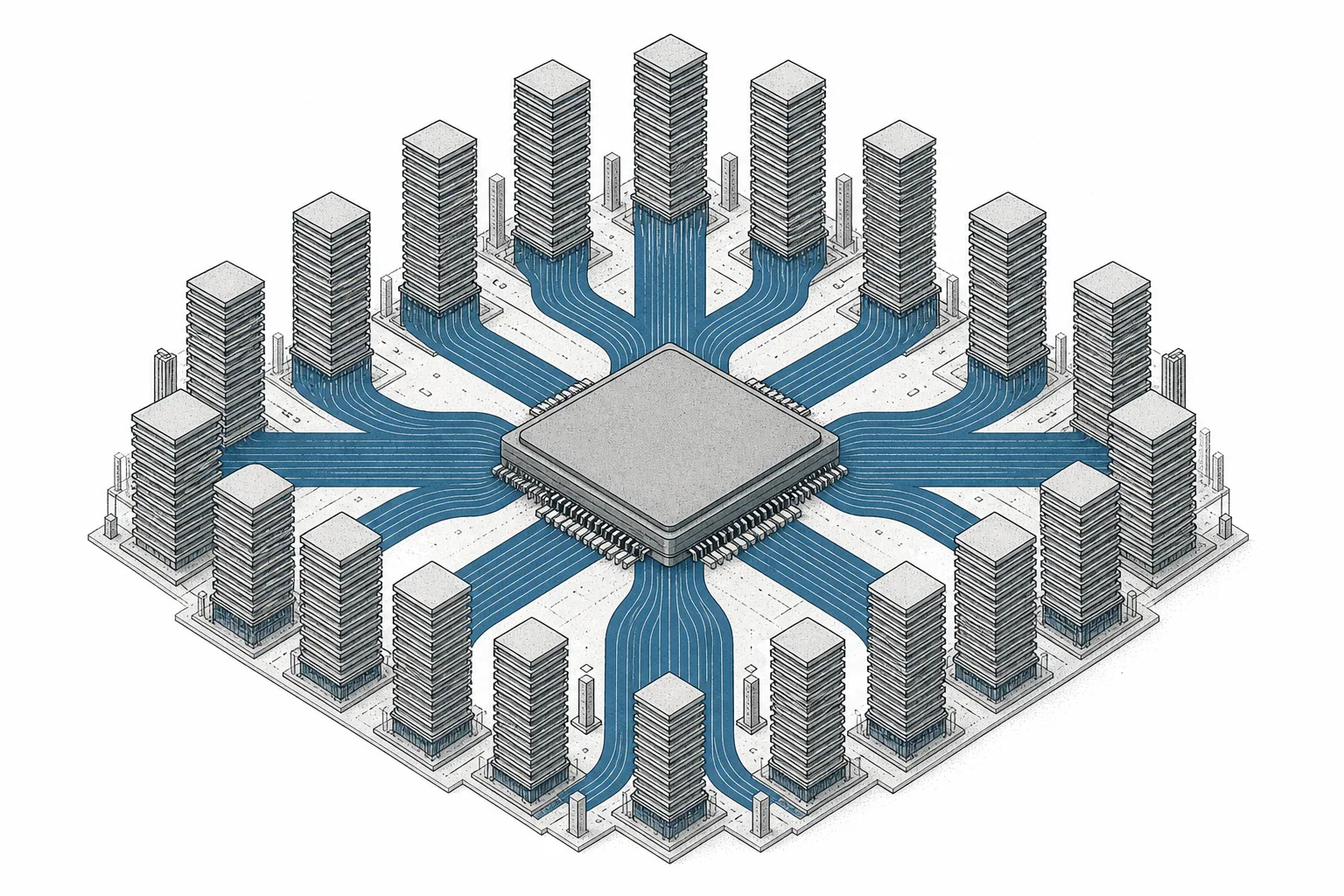
When we talk about the power of AI, we usually picture the GPU computing at top speed. But think about it — no matter how fast a chip computes, it's useless if the "data" to compute on doesn't arrive in time. Like a brilliant chef who cooks blazingly fast: if the person bringing the ingredients is slow, the chef just stands and waits. HBM (High-Bandwidth Memory) was born to solve exactly this — it's ultra-high-speed memory that stacks many layers of DRAM into a tower and slaps it right next to the GPU, to bring the ingredients (data) to the processing core as fast as possible.
Its heart is just two words: "stack" and "wide." Instead of laying DRAM chips out flat on a motherboard like ordinary computer memory, HBM stacks the DRAM wafers 8–16 layers high into a tower, then drills electrical connections straight through every layer. It then places that tower right beside the GPU, connected by a hugely wide "freeway." The result: data travels from memory into the chip dozens of times faster than ordinary memory.
On the megatrend map, this node is a leaf under AI Compute & Accelerator Silicon, in the big trend Artificial Intelligence. It stands alongside siblings like GPU & Merchant Accelerators (the part that thinks) and Advanced Packaging & Test (OSAT) (the one that assembles the GPU and HBM together) — if the GPU is the brain, HBM is the short-term memory sitting right next to it, letting the brain keep thinking without having to stop and wait.
Bandwidth = how much data can be sent per second — measured in GB/s or TB/s. The more, the faster you can feed data · DRAM = the main memory chip that holds data while you work (your computer's RAM is DRAM) · HBM = many DRAM wafers stacked into a tower and joined by an extra-wide bus, to get the maximum bandwidth in the smallest space — it's a kind of DRAM, just arranged specifically for speed.
02Why it matters — the memory wall
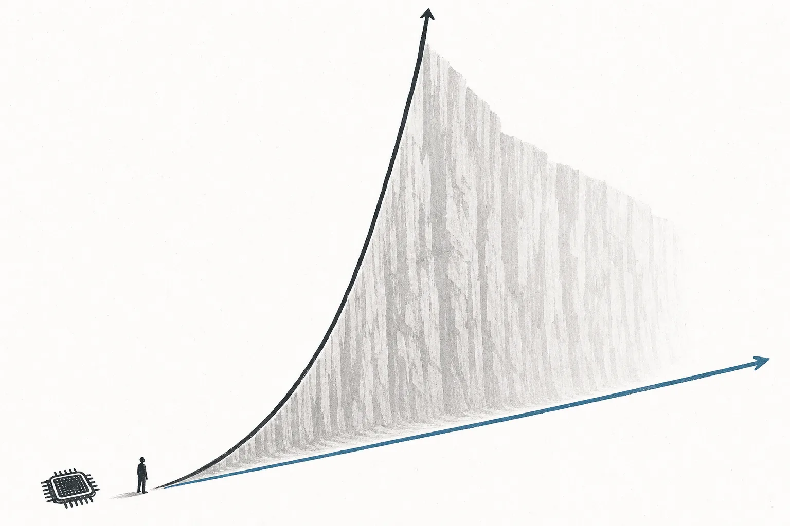
There's a phenomenon that has haunted the chip industry for years, called the "memory wall." Here's the story — the processing power of GPUs is growing far faster than the speed of memory. The number often cited: between 2012 and 2022, the compute power (FLOPS) of Nvidia GPUs rose about 80×, but memory bandwidth grew only about 17×. That gap widens every year, until memory became the number-one "bottleneck" — the most expensive core on the card often sits waiting for data instead of thinking.
This gets even more severe in modern AI work, especially running large language models (LLMs). Every time the model answers a question, it has to read hundreds of billions of parameters from memory. This kind of work "eats" bandwidth more than it eats compute power — so how fast ChatGPT responds is set by the speed of the memory more than the speed of the thinking core. HBM is the only thing that can feed data fast enough to keep up with the GPU's hunger, so it isn't an add-on — it's an indispensable part.
The size of the market reflects this importance clearly. From being just a niche memory worth a few billion, the HBM market surged to about $35 billion in 2025, and many houses estimate it will reach $100 billion by 2028 — growing about 40% a year on average, one of the fastest-growing chip markets in history.
03How it works (stacking DRAM into a tower)
HBM's trick is to change direction from "laying flat" to "stacking vertically." Ordinary computer memory plugs in side by side on the motherboard and talks to the chip through narrow wires (DDR5 is 64 bits wide per channel). But HBM does three different things — it stacks DRAM wafers into a tower, drills connecting holes through every layer, and places that tower right next to the GPU on the same base. Let's walk through it step by step.
The secret is "wide," not "fast per wire." Instead of pushing each wire's data to run as fast as possible (which runs hot and burns power), HBM opens up an enormously wide path instead — one tower has a bus 1,024 bits wide (HBM3) up to 2,048 bits (HBM4), versus DDR5 at just 64 bits per channel. It's like turning a single-lane road into a 16–32-lane freeway: cars move at a moderate speed, but a huge amount gets through at once. The result: one HBM3E stack sends about 1.2 TB per second, and high-end AI cards usually place 8 HBM stacks, multiplying total bandwidth several times over.
TSV (Through-Silicon Via) = a tiny hole drilled through every DRAM layer and plated with metal, so signals can travel straight up and down between layers — the reason stacking layers can still be fast · Interposer = the silicon base on which the GPU and the HBM tower sit together, acting as a "freeway" that routes thousands of wires to connect the two sides at very close range — and this entire assembly step is the job of Advanced Packaging & Test (OSAT).
04Where it sits in the AI ecosystem
HBM doesn't work alone. It's one part that has to be assembled together with its neighbors in the AI chip chain, inseparably. Let's see who it connects with.
- Always paired with GPU & Merchant Accelerators: HBM was born to feed the GPU. An AI card like Nvidia's Blackwell B200 comes with HBM3E 192GB delivering 8 TB/s of bandwidth — sold as a single package. Without good enough HBM, even the strongest GPU can't perform at full tilt
- Depends on Advanced Packaging & Test (OSAT) for assembly: placing the HBM tower next to the GPU on an interposer takes advanced packaging techniques (like TSMC's CoWoS), which is itself another bottleneck — sometimes there's enough HBM, but not enough assembly capacity
- A branch of Memory in Semiconductors: HBM is a premium kind of DRAM. When makers pour production capacity into HBM (which eats about 3× the wafer per GB of DDR5), it ripples through to memory prices across the whole market — so AI demand pushes up PC and server memory prices too
- Drives demand for Energy Transition & Power Demand and depends on Critical Materials & Supply Chain: AI data centers packed with HBM consume enormous power, and making HBM takes large amounts of specialized materials and equipment
05Where it stands now
The reason HBM is always in the news is that it's sold out years in advance. That's no exaggeration — in mid-2025, SK Hynix's finance chief stated plainly that the company "has sold out all of its 2026 HBM capacity." Micron likewise confirmed that its 2025 and 2026 capacity is fully booked. When something is this scarce, prices jump — Samsung and SK Hynix raised HBM3E prices for 2026 by about 20%, while ordinary server DRAM prices got pulled up along with it.
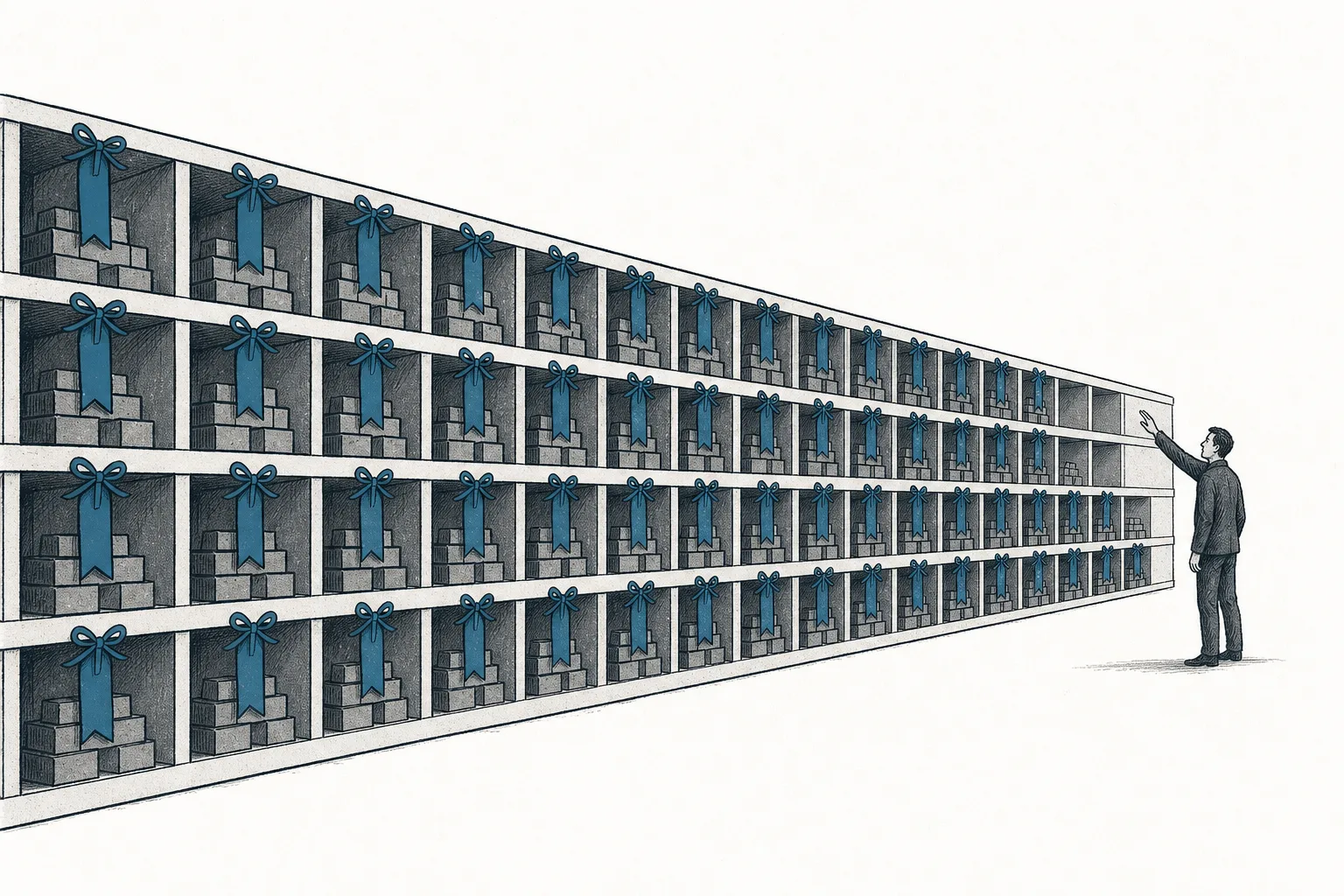
But the more shocking picture is the concentration — nearly all of the world's HBM comes from just three makers, and within that, one single maker controls most of the market. SK Hynix holds about 60% of the HBM share in 2025 and grabbed about 70% of Nvidia's HBM4 orders. Behind it are Micron and Samsung, swapping the number-two spot each quarter.
Why is it so hard for newcomers to get in? Because HBM is far harder to make than ordinary memory. Stacking 12 layers of DRAM means grinding each wafer paper-thin (about 10–20 microns), then drilling TSV holes that line up across every layer without bending — work with low yield (the share of good units) that's easy to botch. Each GB of HBM eats about 3× the wafer of DDR5 — the accumulated know-how and experience become a high wall, so high that even Samsung once stumbled on the HBM3E round and got overtaken.
The main tailwind is AI demand that shows no sign of stopping. Because Nvidia, AMD, and the tech giants that design their own chips (Custom Silicon / ASIC) all need HBM, all three makers keep setting new records for revenue and profit — HBM has become a "gold mine" that flipped the memory business from a volatile commodity into a premium product customers have to queue for.
06The future — HBM4 and a smarter base
The first direction is the move to HBM4, which JEDEC ratified as a standard in April 2025, with real shipments starting in late 2025 to early 2026. The big shift is the bus doubling in width (2,048 bits per stack), bringing bandwidth per stack to about 2 TB/s, with up to 16 layers (48GB per stack). The first customer is the Nvidia Rubin card, which will place up to 8 HBM4 stacks for a total of 288GB of memory and total bandwidth of about 22 TB/s per card.
The second direction is more interesting — HBM is ceasing to be a commodity and becoming a made-to-order product (custom HBM). The heart of it is the "base die," the bottom layer of the HBM tower. It used to be just a connector, but in HBM4 it gets upgraded to a real logic chip made with TSMC's advanced technology (from 12nm down to 3nm). This lets chip designers "embed" the memory-control circuitry into the base die — meaning the memory is designed for that specific GPU, no longer an off-the-shelf part you buy and plug in.
This changes the very definition of the memory business — from selling the same thing and competing on price, to "co-designing with the customer." That binds HBM makers more tightly to big customers like Nvidia, giving them more bargaining power and higher profit per unit — and making it even harder for new players to compete.
07Challenges & risks
The first risk is extreme concentration, on both the seller and the buyer sides. There are only three sellers, and one controls over half. The buyer side is heavily concentrated too — Nvidia alone absorbs most of the world's HBM demand. When the whole chain depends on a handful of companies, if any one stumbles (yield drops, a factory problem, or a big customer slows its plans), the shock spreads through the entire AI industry instantly.
The second risk is the memory cycle. The DRAM business is famous for swinging up and down in strong waves. When demand surges, prices soar and everyone races to add capacity. But when all that capacity floods the market at once, prices plunge. Right now HBM looks like a "gold mine" sold out years ahead, but if all three makers expand capacity too aggressively, or AI demand slows even temporarily, the downturn could return — today's record profits aren't guaranteed to last forever.
The third risk is mounting technical difficulty. The higher you stack (12 layers to 16 layers), the more heat builds up inside the tower, while the tower's total height is capped by the standard (about 720–775 microns) — meaning each wafer has to be ground even thinner without bending or cracking. Every new generation pushes the limits of physics — whoever achieves yield first gains a huge edge, and whoever stumbles can lose a big customer for that entire round, as has happened before.
In short: HBM is memory that stacks DRAM into a tower and slaps it next to the GPU to break the "memory wall" — a part sold out years in advance, with fat profits and a high wall, but concentrated and swinging with the cycle. Every time AI gets smarter and hungrier for data, the role of "the one who feeds the brain" grows that much more important.