Megatrend · Semiconductors
The final step that became the AI era's bottleneck
For decades, 'chip assembly and test' was the final step nobody cared about — back-office work, cheap, anyone could do it. Then AI suddenly turned it into the world's real bottleneck. Because building a single AI chip is no longer just about making the chip smaller — it's about 'packaging' several chips together with HBM memory into one block. And today, NVIDIA has booked this very step at TSMC solid through 2027.
01What it is (OSAT and advanced packaging)
When we talk about 'making chips,' most people picture an ultra-advanced fab printing circuits onto silicon — that's the work of a Foundry. But here's the thing: once the silicon (wafer) comes out of the fab, it's still useless. It's just a round disc with hundreds or thousands of raw chips lined up on it. Someone has to cut it into individual chips, wrap each in a 'package' with legs so it can plug into a board, and test which ones are good and which are bad. This back-office step is the heart of this lesson.
The industry calls the companies that do this work OSAT (Outsourced Semiconductor Assembly and Test) — literally 'outsourced chip assembly and test.' It's exactly like the foundry model but at the other end: chip designers and foundries don't want to invest in their own assembly-and-test equipment, so they hand it off to an OSAT. Companies like Taiwan's ASE or America's Amkor are the subcontractors at the tail of this production line.
The chip world splits work into two sides · Front-end = building transistors onto the wafer (the foundry's job, using EUV machines, the most advanced and expensive part) · Back-end = taking the wafer, cutting it, assembling it into packages, and testing (the OSAT's job). For a long time back-end was seen as the 'boring, cheap step' tacked onto the real work — but AI is flipping that belief.
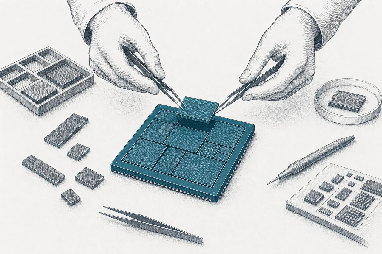
But the interesting part is the word 'advanced' packaging. Packaging used to mean just dropping a single chip into a plastic box and running legs out — easy work, thin margins. But advanced packaging means assembling several chips together in one package so they talk to each other as fast as if they were one chip. The star of this era is a technology called CoWoS from TSMC, used to join NVIDIA's AI chip with HBM memory — and it's the bottleneck the whole world is fighting over right now.
On our megatrend map, this node is a sub-branch under Semiconductors, and it's the 'final gate' before a chip ships into real AI servers — the gate that suddenly became the narrowest in the entire production line.
02Why the final step became the bottleneck
It starts with a physics problem — Moore's Law is slowing down. For decades the chip industry got better by making transistors ever smaller, packing more onto a single chip. But now shrinking further is hard and hugely expensive. There's also the 'size wall' (reticle limit) — a physical limit on how big a chip the circuit printer can make. Power-hungry AI chips hit this ceiling and can no longer be built as a single block.
The solution was a change in thinking: instead of making one chip bigger and more advanced, take several small chips (called chiplets) and assemble them together to work as one. This all happens in the packaging step. Put another way, chip progress moved from the 'front-end (making it smaller)' to the 'back-end (assembling it better).' That's why a once-boring step became the new battleground.
Chiplet = a small chip designed for a specific job (a compute die, an I/O die) that you combine several of in one package into a powerful system · The upsides: easier to make (smaller dies yield better), you can mix technologies from different generations, and you can break past the reticle limit · Almost all new AI chips are chiplets — NVIDIA's Blackwell (B200), for instance, is two chips joined together.
And this is a big, fast-growing market. The global OSAT market sits at around $46–47 billion in 2025 and is expected to reach ~$100 billion by 2035 (about 8% annual growth). But the truly hot engine is the advanced packaging segment, which grows far faster — and the hottest part, chiplets, is projected to grow from ~$52 billion (2025) to ~$157 billion (2030), about 25% a year.
03How CoWoS works
Picture a single AI chip powering ChatGPT. It isn't one block — it's a processing chip (GPU) in the center, surrounded by several stacks of HBM memory. Everything has to sit as close together as possible to move data at extreme speed. The question is — how do you place separate chips, made in separate fabs, side by side so they communicate with nanometer precision?
The answer is CoWoS (Chip-on-Wafer-on-Substrate), a TSMC technique. Its heart is a thin layer in the middle called an interposer — a silicon sheet that acts as a 'high-speed bridge,' with ultra-fine wiring connecting the GPU to every HBM stack. Instead of running long wires across an ordinary board (slow), everything sits on the same silicon bridge (vastly faster).
So why is it so hard that it becomes a bottleneck? Because the interposer is itself a piece of silicon that must be made in a foundry-grade fab, and placing several chips onto it with every one of its tens of thousands of joints aligned perfectly — not a single one allowed to miss — is exquisitely delicate work. One bad joint and a tens-of-thousands-of-dollars AI chip is scrapped whole — which is why capacity expands slowly and costs run high.
2.5D = placing several chips 'side by side' on an interposer (e.g. CoWoS — GPU and HBM on the same plane) · 3D = 'stacking' chips vertically and connecting through them with TSV holes (e.g. TSMC's SoIC — stacking processing chips directly) · 3D offers higher density and speed but is far harder, because you have to cool stacked chips — it's the industry's next direction.
04How it connects in the ecosystem
This node is the 'convergence point' where every part of an AI chip actually comes together into one block. So it's tightly linked to both its siblings in the chip world and the trends downstream:
- Feeds AI directly and most intensely: every AI chip passes through this step — no advanced packaging, no modern GPU. The entire AI boom runs through this bottleneck.
- Partnered with Memory (HBM): CoWoS exists precisely to join the GPU with HBM, so the HBM bottleneck and the packaging bottleneck are tightly intertwined — a shortage of one drags the other.
- The line with Foundry is blurring: foundries used to make the wafer and hand it to an OSAT to package, but now TSMC does CoWoS in-house and keeps the most advanced part (the interposer) — making TSMC the largest and most profitable OSAT too, leaving external OSATs only the 'overflow' work TSMC can't handle.
- Sits on Interconnect & substrate: beneath the interposer is an advanced substrate (ABF substrate), a critical part that has been in shortage before.
- Opens the way for Cloud, electric vehicles and robots: every trend that needs high-performance chips leans ever more on advanced packaging.
05Where it stands now
The story that dominated the news all through 2025 was the 'CoWoS shortage'. AI-chip demand outran packaging capacity, so TSMC went all-out expanding CoWoS — from ~35,000 wafers/month at the end of 2024 to ~75,000/month in 2025, targeting 120,000–130,000 wafers/month by the end of 2026, nearly a 4x increase in under two years. The astonishing part — even that isn't enough.
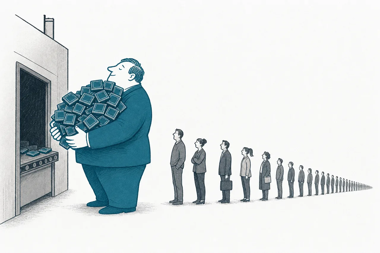
The reason it's still not enough is that NVIDIA has booked nearly all of it. NVIDIA is reported to have already reserved more than 50% of TSMC's 2026 CoWoS capacity (some put it above 60% counting 2025–2026), about 800,000–850,000 wafers for 2026 from a single customer. That forces rivals like AMD and Broadcom to fight over what's left, and CoWoS lead times have stretched past 18 months.
And because TSMC can't keep up, the overflow flows down to external OSATs, making 2025 a banner year for them too. In Counterpoint's 'Foundry 2.0' framework, the OSAT group grew about 10% in 2025, with ASE rising to the second-largest player after TSMC, and Amkor signing a 10-year capacity deal with TSMC at its Arizona plant (Oct 2025) to take on packaging work in the US.
As for the competitive picture, the order is clear: ASE is the runaway leader among external OSATs, followed by Amkor and a fast-rising Chinese group powered by state support:
06The road ahead
The first direction is clear: value is moving from front-end to back-end. As shrinking transistors nears its ceiling, future chip progress will come more and more from 'how you assemble.' TSMC, Samsung and Intel are each pouring tens of billions into expanding packaging capacity through 2027 — the first time in history that the 'back-office' step has become a primary investment arena.
The second direction is the move from 2.5D to 3D. Today's CoWoS places chips side by side (2.5D), but the next step is 'stacking' processing chips vertically (3D, like TSMC's SoIC) to pack more power into the same area — far harder, because you have to cool stacked chips, but it's where NVIDIA and AMD are heading.
The third direction is a common standard for chiplets (UCIe). If chiplets from different companies can talk through one standard (like USB for chips), the market opens up enormously. Anyone could mix chiplets from several makers into their own chip — pushing packaging demand higher still, and possibly decentralizing power away from a few big players.
07Challenges & risks
The appeal of advanced packaging comes with its own specific risks worth understanding.
The first risk is extreme dependence on AI and a few customers. CoWoS's boom today is tied to AI-chip demand and essentially one customer (NVIDIA has booked over half). If AI investment slows or chip architectures change, the nearly-4x capacity expansion could turn into a glut overnight — the cyclical nature baked into the chip industry.
The second risk is most of the value gets pulled up to TSMC. Even though the whole node is booming, the most profitable steps (interposer, chip-on-wafer) TSMC keeps in-house, leaving only the overflow and thinner-margin parts (substrate assembly, test) to external OSATs. So an 'OSAT boom' doesn't mean every player profits equally — you have to be clear about who sits at the most advanced part of the chain.
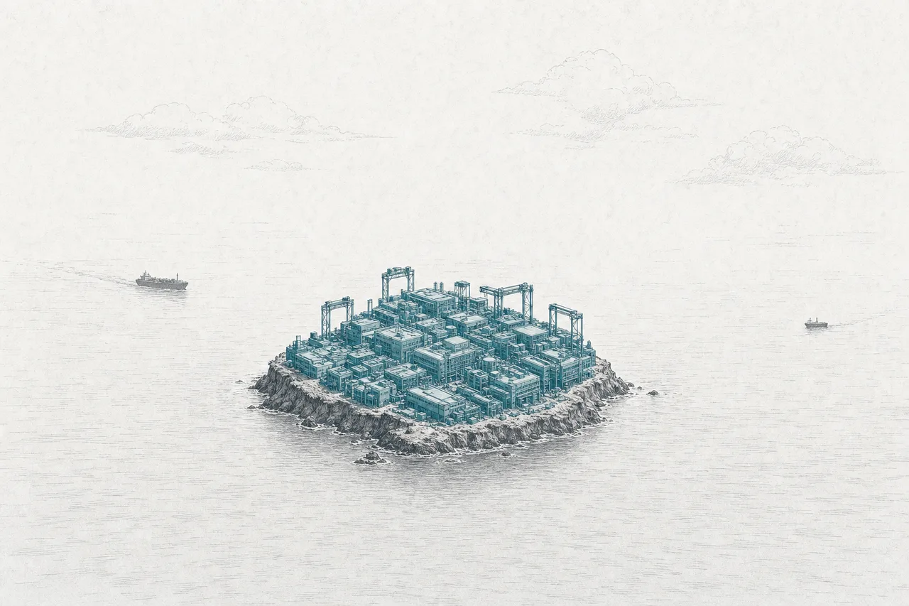
The third risk is geopolitical concentration. Like foundry, almost all top-tier packaging is in Taiwan. Efforts to pull it back to the US (Amkor + TSMC in Arizona) are just beginning, slow and costly. Meanwhile China is racing to build its own OSATs (JCET, Tongfu) for self-reliance — turning a step once seen as 'unimportant' into yet another geopolitical battlefield.
The fourth risk is ever-rising costs. 2.5D advanced packaging costs about 20–30% more than the old style, and makers are raising prices (ASE +5–20%, memory packages up to +30% in 2026). That cost ultimately lands in the price of AI chips and devices — an inflationary pressure across the whole tech chain.
In short: advanced packaging is a lesson that in technology, the most overlooked step can become the most important one when the rules of the game change. When Moore's Law slows, 'how you assemble' matters as much as 'how you make' — and understanding why a single AI chip has to wait in line for packaging for a year is understanding why a back-office step nobody ever cared about became the bottleneck setting the speed of the entire AI era.