Megatrend · Semiconductors
The thousands of tiny parts AI can't do without
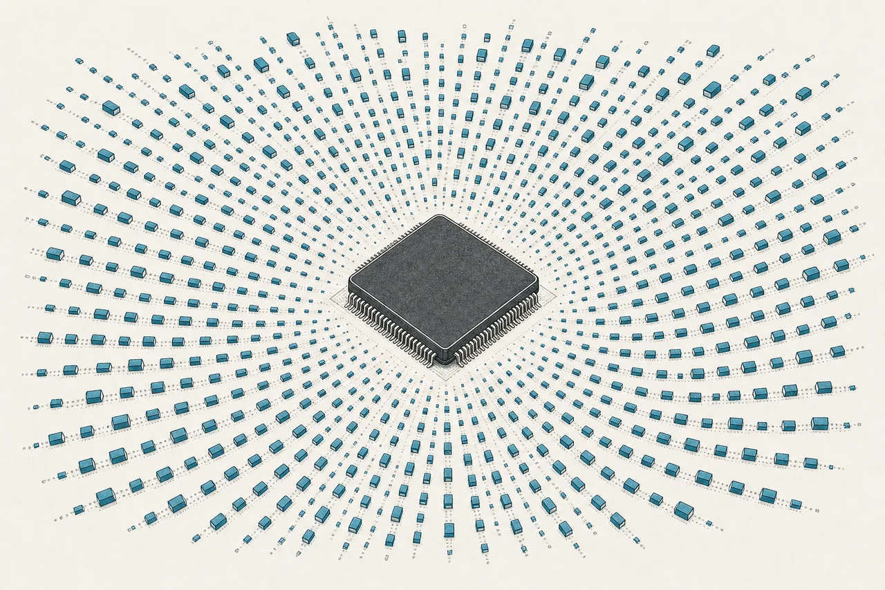
Everyone talks about the expensive GPU chip, but a single chip does nothing on its own — it only works thanks to the thousands of 'supporting actors' around it. Tiny capacitors, the circuit board, and the substrate the chip sits on. One AI server uses 2,000–5,000 of these parts, and they're turning into a new bottleneck and a new supercycle.
01What it is
Open up your phone and look. You'll see a few chips — but what you don't see is roughly 1,000 more tiny black parts the size of a grain of sand, scattered across the board. These are the 'passive components' and the underlying structure that ties everything together — this node is about them.
They split into three groups, which are this node's three sub-themes — picture them as 'layers' holding the chip up:
- Passive Components: capacitors (especially the MLCC), inductors, resistors — they tune and steady the power. A chip can't run if the power isn't clean
- PCB (printed circuit board): the 'roads' that connect the chip and every component — the biggest market of the three (around $95 billion). The more complex the chip, the more layers you stack (AI servers use 18 layers and up), which is where the higher value comes from
- CCL & Substrate (board materials and substrate): the raw material for PCBs, and the special 'substrate' the AI chip sits on directly (like ABF substrate)
MLCC (Multilayer Ceramic Capacitor) = a tiny ceramic capacitor, smaller than a grain of sand, that stores and releases power to steady a circuit. It's the most-produced component in the world · Passive = a part that doesn't 'think' or amplify a signal (capacitor/resistor/inductor), unlike an active part such as a chip or transistor that can process — but without passives, actives can't work.
On the megatrend map, this node sits under Semiconductors as a 'supply-chain layer' around the chip. If Foundry is the one who builds the chip, this node is the one who makes everything around the chip so it actually works.
02Why the 'boring' stuff became a big deal
These parts were seen as boring for a long time — cheap, commodity, nothing to get excited about. But the AI revolution is changing everything, because AI servers are a huge 'eater' of these parts.
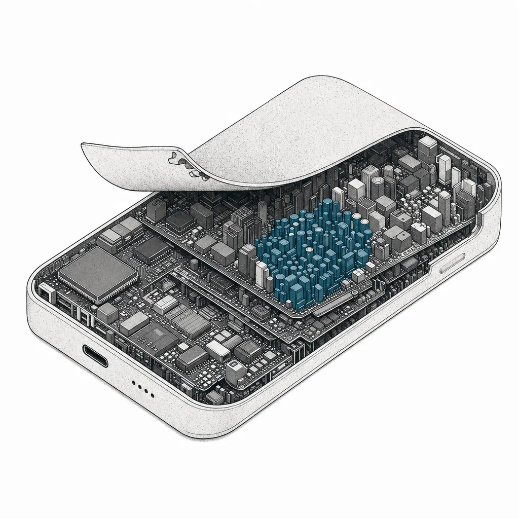
The 'parts per device' count is climbing everywhere, not just AI — a new EV (especially 800-volt systems) uses up to about 10,000 MLCCs per car, versus roughly 1,000 in a phone.
And it's a much bigger market than people think. Look at the size of each layer around the chip — together it's serious money:
Some analysts are even asking whether MLCCs could become the 'next HBM' — meaning a part once overlooked that suddenly goes short and spikes in price on AI demand, just as HBM memory did.
03How it works (the layers around the chip)
The best way to understand this node is to see it as 'layers' holding the AI chip up. The chip doesn't just float — it sits on a complex, multi-layer structure, and each layer is one of this node's sub-themes.
The challenge is that 'the high-end stuff is very hard to make.' An AI chip that draws enormous power and moves data at extreme speed needs a precise ABF substrate, a PCB that stacks 18 layers and up, and MLCCs that hold high charge in a tiny size — only a handful of companies in the world can make these, and that's where the bottleneck comes from.
ABF substrate = a high-density substrate that a large chip (especially an AI chip) sits on, connecting the chip's tens of thousands of pins to the PCB — a key bottleneck in assembling AI chips · HDI (High-Density Interconnect) = a high-density PCB that packs fine traces and stacks many layers, used in flagship phones and AI servers.
04How it connects in the ecosystem
This node is the 'connective tissue' that ties the chip to everything — it feeds almost every trend that uses electronics:
- Feeds AI directly: AI-server demand is the new engine for the whole group — multi-layer boards, substrates, and tiny capacitors all benefit at once
- Sibling to Foundry and OSAT: the line between 'substrate' and 'chip packaging' is blurring — ABF substrate is where the world of PCBs meets the world of AI-chip assembly
- Opens the way for EVs and robots: electric vehicles and automation systems use enormous passive content per unit, especially heat- and high-voltage-rated grades
- Depends on key raw materials: from ceramic powder, copper and gold to specialty resins — making costs very sensitive to material prices (in 2025, surging gold and CCL prices squeezed the whole chain)
05Where it stands now
We're at a point where AI demand is 'upgrading' the whole industry — not just selling more parts, but selling more of the pricier high-end stuff. And that's where the profit is.
It's clearest on the PCB side — while ordinary PCBs grow at a normal pace, multi-layer PCBs (18 layers and up) for AI servers are surging around 62%, and HDI is up about 14%, showing the money piling into the high end.
Another hot battleground is ABF substrate, the bottleneck in AI-chip assembly. This market is highly concentrated — just 5 makers (Unimicron, Ibiden, AT&S, Nan Ya, Shinko) hold 74% combined and are racing to add capacity, with Japan's Ibiden pouring over $3.3 billion into more substrate capacity for AI servers.
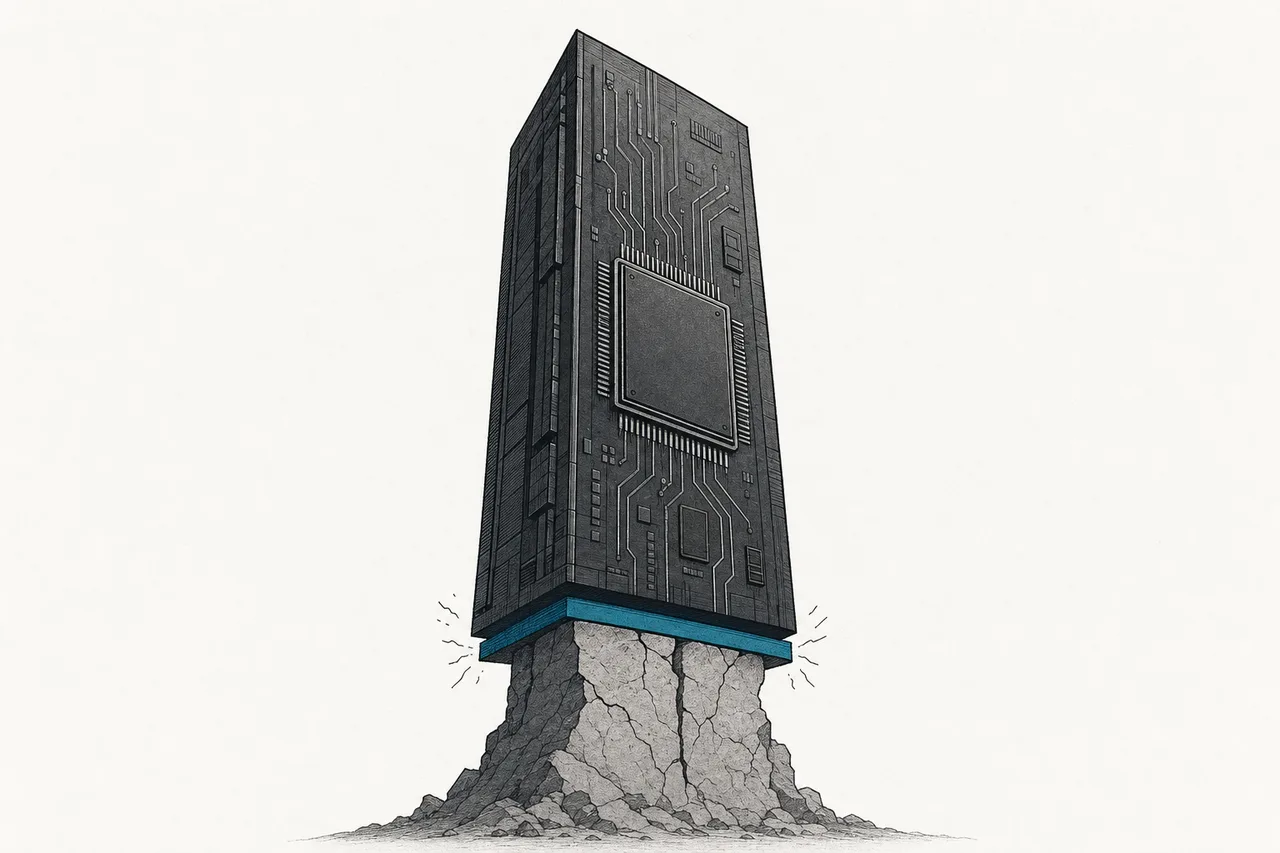
On the materials side (CCL), 2025–2026 brought a 'price storm' — gold and high-grade CCL prices surged, pushing high-end CCL makers to raise prices around 30–50% one after another (deep dive in CCL & Substrate Materials).
06The road ahead
The first direction is that 'parts per device' keeps rising. Everything that gets smarter (AI cars, robots, servers) needs more passive components and more interconnect. Murata even projects that MLCC demand from AI servers will grow 3.3× in 5 years — a clear long-term tailwind.
The second direction is that the 'substrate' becomes a key battlefield. As AI chips get bigger and more complex, ABF substrate and new substrate technologies (like the glass substrate in development) become a bottleneck and a new source of value — whoever controls this holds real bargaining power.
The third direction is moving up to the high end. Players stuck on cheap commodity parts get squeezed, while those that move up to AI/automotive grade get both better demand and better margins — the future game is 'escape the price war, head for the hard-to-make stuff.'
07Challenges & risks
This node's appeal comes with its own specific risks you have to understand.
The first and biggest risk is 'the most brutal cycle in the industry.' Passive components and PCBs swing hard with the electronics cycle — short and spiking in good times, glutted and crashing in bad ones. Makers that expand capacity at the peak tend to get hurt badly when the cycle turns.
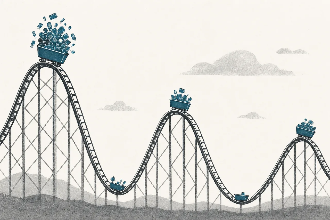
The second risk is a two-tier market. The low end (ordinary MLCC/PCB) is a commodity that China is overproducing, heavily pressuring prices and profits. The high end (AI/automotive grade, ABF substrate) is short and richly profitable — the same company can hold both a growing business and one being squeezed, so reading this trend means telling exactly who sits in which tier.
The third risk is dependence on raw materials and concentration. Costs are very sensitive to copper, gold and specialty-resin prices (the 2025 price storm is the example), and the high-end technology is concentrated mainly in Japan and Taiwan — so supply-chain and geopolitical risk runs underneath.
In short: this node is a reminder that the greatest technology often depends on the smallest, most boring parts — and in the AI era, these 'boring' things are becoming both a bottleneck and an opportunity. Understanding the layers around the chip is understanding why, sometimes, a whole industry's crisis starts with a part smaller than a grain of sand.