Megatrend · Semiconductors
A million-dollar AI chip sits on a "board" that's as hard to make as the chip itself
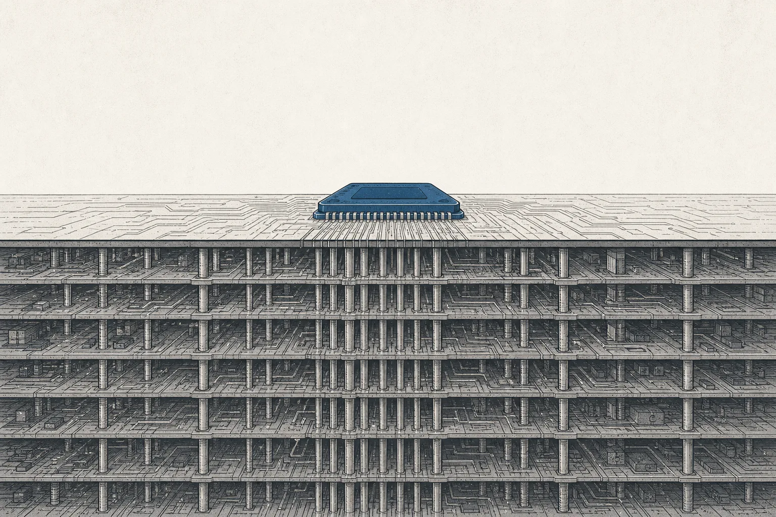
We talk about NVIDIA's GPUs all the time, but a GPU alone does nothing without the green board every part plugs into. The printed circuit board (PCB) is the "roads and bridges" that carry power and signals between the thousands of chips on a single AI server. As chips get faster and hotter, this board stacks up more layers — from 8 to 40–60 — drills holes thinner than a hair, and uses special materials that cost many times more. It's a market worth nearly $100 billion a year, more than 80% of it made in Asia, and it has quietly become a bottleneck of the AI era.
01What it is
Open up any computer, phone, or TV and you'll find a "green board" covered in copper traces running everywhere. That's the printed circuit board (PCB) — the base that holds every electronic part together. More importantly, it's the "road" that carries electricity and signals between each chip. If the chip is the brain, the PCB is the system of blood vessels and nerves connecting every part of it.
This node is specifically about the makers of PCBs — the rigid kind inside computers, the flex kind that bends into tight corners in phones, and the star of this era, HDI (High-Density Interconnect) — high-density boards that pack in many times more signal paths than usual, with traces and connecting holes smaller than 152 micrometers (some as narrow as 75 micrometers — thinner than a human hair). This is the kind flagship phones and AI servers need.
On the megatrend map, this node is a branch under Interconnect & Passive Components within the big trend Semiconductors. It sits in the "supply chain" layer — the maker of the base board every device must have. Its siblings next door are Passive Components (the MLCC capacitors that plug onto the PCB) and PCB Laminates & Substrate Materials (the CCL material the PCB is made from) — these three are the "floor and frame" holding up every chip.
PCB = the base board with copper traces connecting the parts · HDI = a high-density PCB with especially fine traces and holes · Via = a small copper-plated hole drilled through to connect signals between layers — HDI uses a laser-drilled "microvia" about 75–100 micrometers across · IC Substrate = an even finer board sitting directly under the chip — the finest relative of all, but split off into its own node (IC Substrates). This node is about the big board the whole chip package sits on.
02Why it matters — the board AI must sit on
We tend to think the AI battle is a battle of chips — who makes the fastest, most powerful GPU. But the truth people overlook is that no matter how powerful an AI chip is, it's worthless if data can't move in and out fast enough. And the thing that "keeps the data moving in time" is the very PCB beneath the chip. One AI server rack has thousands of chips that must talk to each other at speeds of 800 gigabits per second and up — and making a board that can handle that speed is enormously hard.
The size of the market reflects this importance. The global PCB market was worth about $95.8 billion in 2025 and is expected to reach $127 billion by 2031, growing about 4.8% a year. But that total hides a truth: the part that grows fast and makes good money is high-end boards for AI and 5G, not the ordinary boards in consumer electronics.
The reason AI pushes this market is clear: one AI server uses a board stacked 40–60 layers deep (versus a few layers in an ordinary machine), packed with microvias and heat-dissipation holes — sending the price per board past $200, about 4 times more than an older server board. In 2025, cloud providers worldwide installed about 1.2 million AI servers, each one holding several high-end boards. This is a whole new wave of demand that appeared in just a few years.
And it's not just AI — one electric vehicle (EV) carries about $150–200 worth of PCB inside it, roughly double a gas car, because it's packed with battery-control systems, sensors, and displays. Demand from AI, 5G, and EVs together has made the PCB a basic component every megatrend depends on.
03How it works (built layer by layer)
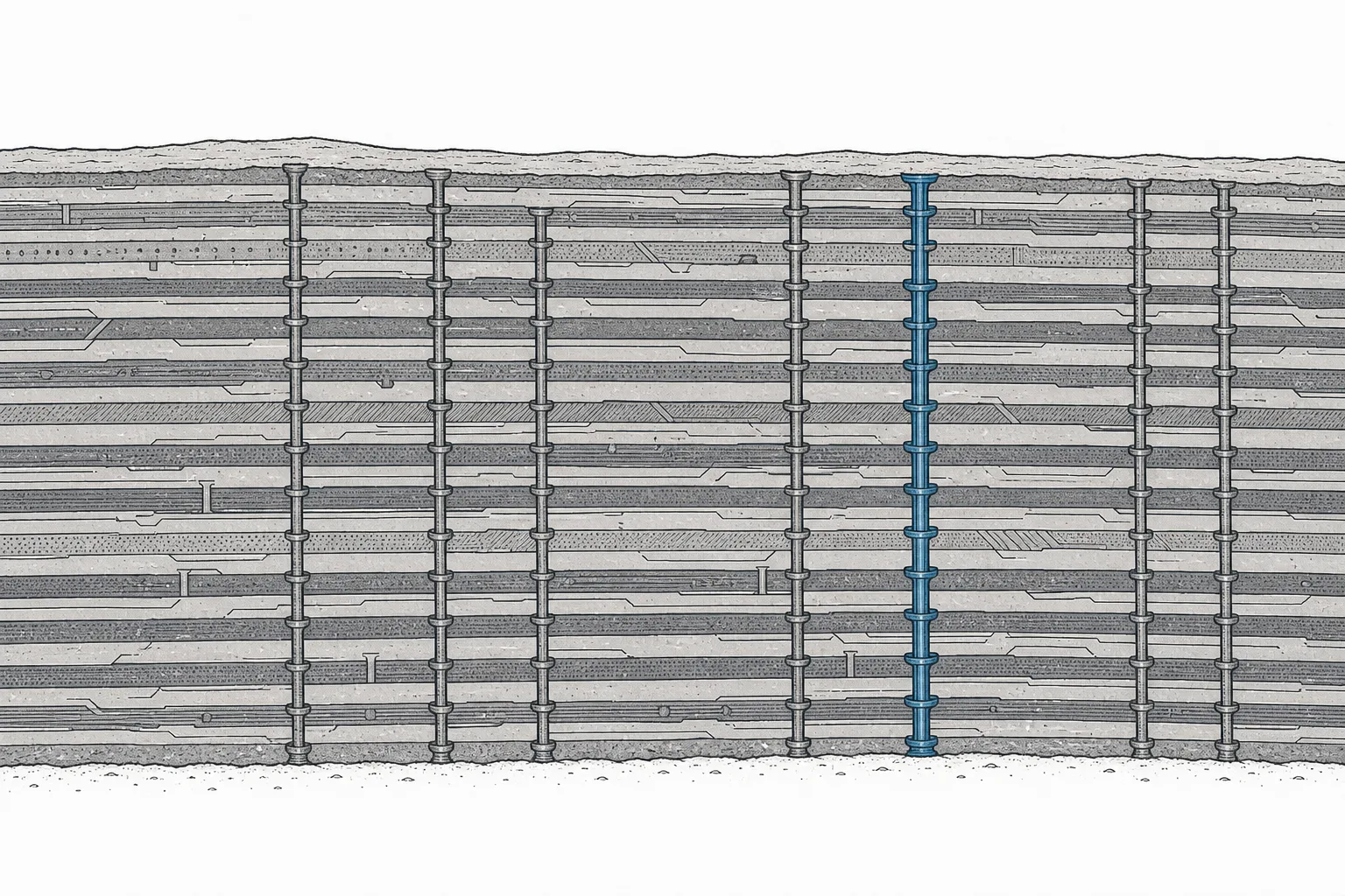
Many people think a PCB is a single board with traces stamped on. But in reality, high-end boards are built up one layer at a time — like a multi-layer cake. Each layer has its own copper traces, then they're pressed together. Let's walk through, step by step, how a single board comes to be.
Here's exactly what makes an AI board "hard": when you have to stack 40–60 layers, every layer has to line up to within micrometers. Shift even slightly and a via drills off-target, ruining the whole board. And when signals run at 800 gigabits per second, the board material has to be especially "low-loss" — these special materials are expensive, only a handful of firms can make them, and they've become yet another bottleneck in the chain.
04Where it sits in the chip world
If you picture the whole electronic system as a body, the chip is the brain and the PCB is the skeleton and blood vessels that hold and feed everything together. It sits right in the middle, between "raw materials" and "final product," connected to several neighbors.
- Needs material from PCB Laminates & Substrate Materials (CCL): a PCB is made from "copper-clad laminate." For high-speed AI boards, this material has to be an especially low signal-loss grade — whoever controls the material controls one of the chain's bottlenecks
- Is the base for Passive Components and chips: MLCC capacitors, resistors, and the chips themselves all plug or solder onto the PCB — the PCB is the stage where every part comes together
- A different layer from IC Substrate: directly beneath the chip is a "chip carrier" (substrate) far finer than an ordinary PCB. This node's PCB is the big board that the chip-plus-substrate then sits on — if the substrate is the "room floor," the PCB is the "building floor"
- Feeds AI · Cloud & Digital Infrastructure · Electrification & Mobility directly: AI servers, data centers, and every EV need this board, and it reaches on to Robotics and Quantum Computing, which all need a board to carry their chips
05Where it stands now
The first thing to know is the concentration in Asia — in 2025, the Asia-Pacific region produced about 82.5% of the world's PCBs. China controls the high-volume boards (mobile HDI, fiercely price-competitive), Taiwan controls the high-end boards and advanced technology, and Japan excels at high-reliability boards for automotive and industrial use. The West has almost no advanced PCB capacity left.
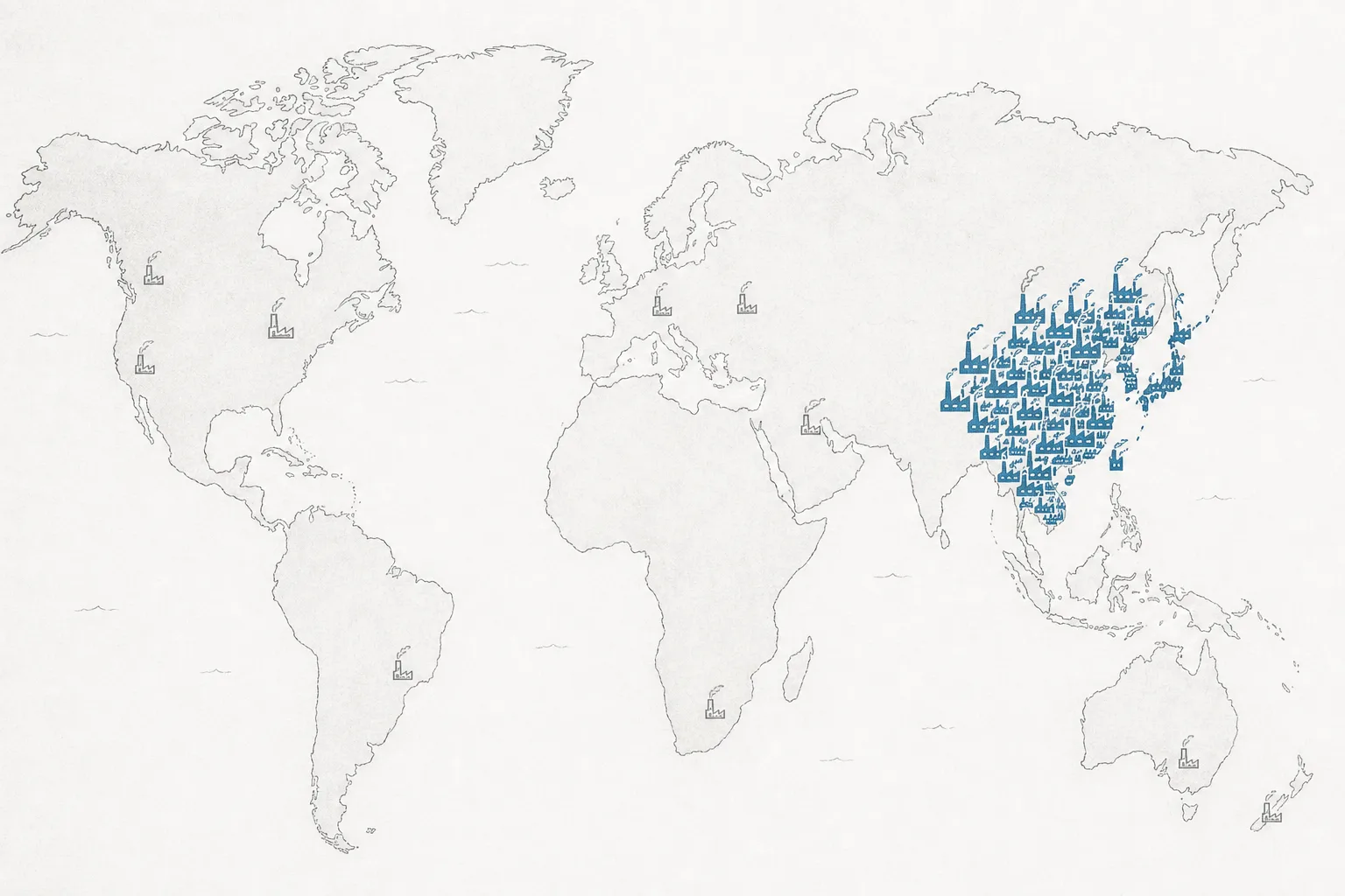
The second is the AI wave reordering the winners. Boards for the GPUs and switches of AI servers need many layers, special materials, and a precision only a handful of factories in the world can manage. The Taiwanese makers who grabbed this work first — especially Unimicron, Nan Ya PCB, and Gold Circuit — have won big orders and are racing to expand capacity. Meanwhile Zhen Ding, the world's largest PCB maker (part of Foxconn, strong in mobile flex boards), is pushing into the AI market too.
The third is China's catch-up. Chinese makers like Shennan Circuits, Victory Giant, and Avary are investing heavily in high-end board production lines and are already entering the supply chains of global AI customers — a market once seen as "easy and cheap" is becoming a serious technology battleground.
06The road ahead
The first direction is more and more layers, more and more expensive materials. Every time a new AI chip gets faster, the board that supports it has to stack more layers and use lower signal-loss material than before. This is a structural tailwind: a maker's revenue grows not just with the "number of boards" but with the rising "value per board" — a board that once sold for tens of dollars becomes one that sells for hundreds.
The second direction is materials become the star. When signals run as fast as 1.6 terabits per second for new optics, ordinary copper board starts to fall short and you need especially low-loss materials — and in some places PCBs are starting to merge with IC Substrate technology, blurring the line between "board" and "chip carrier." That opens a window for makers who can cross over into finer work first to capture a big chunk of added value.
The third direction is spreading out the production base. Geopolitical tension and rising costs in China are pushing makers to expand factories into Thailand, Vietnam, and elsewhere in Southeast Asia — even though Asia still controls the market, the map within Asia is being redrawn, and Thailand itself is one of the destinations where many PCB makers are setting up.
07Challenges & risks
The first risk is sharp cyclicality. The PCB business is tied to the consumer-electronics cycle and data-center investment, which swing up and down in strong waves. In 2023, when the phone and PC markets slumped, many PCB makers saw revenue shrink — before the AI wave came to support them in 2024–2025. It's a business that profits well in a boom but has to endure the slumps that come in cycles.
The second risk is geographic concentration. With over 80% of PCBs made in Asia and most of the high-end in Taiwan and China, any regional tension or trade measure can shake the whole global supply chain instantly. The West, which wants to bring production back, finds that building new advanced PCB capacity takes enormous time and money.
The third risk is price competition and thin margins. Ordinary (non-high-end) PCBs are a product competed on mainly by price, with thin margins and many makers fighting over the same market. Anyone stuck on ordinary work who can't move up to AI/high-end fast enough gets squeezed from both rising material costs and falling prices — the real value lies in "who can move up to the hard stuff," not who can make the most.
In short: this node is the board that holds and connects every chip — it looks like a plain commodity, but as AI chips get faster and hotter, this board turns into harder, more profitable engineering all the time. And the further the world moves toward AI, EVs, and 5G, the more demand there is for a "board good enough" to handle it.