Megatrend · Semiconductors
The stuff that flows into a chip plant before a single chip exists
Everyone talks about TSMC. About NVIDIA. About the $200-million EUV machines. But before any of those machines can run, something has to flow into the plant first — silicon wafers smoother than glass, photoresist purified to one part in a trillion, and dozens of special gases. This is the deepest layer of the chip supply chain: the 'materials.' It looks like a commodity, but it's actually controlled by just a handful of Japanese companies — and it was once used as a 'weapon' in a trade war.
01What it is
Think of making a chip as the world's most complex 'baking.' ASML's EUV machines and TSMC's plants are the oven and the chef everyone talks about. But before you start baking, you need the 'ingredients' first — flour, sugar, butter, which here means silicon wafers, photoresist, and special gases. This node is about all of those materials.
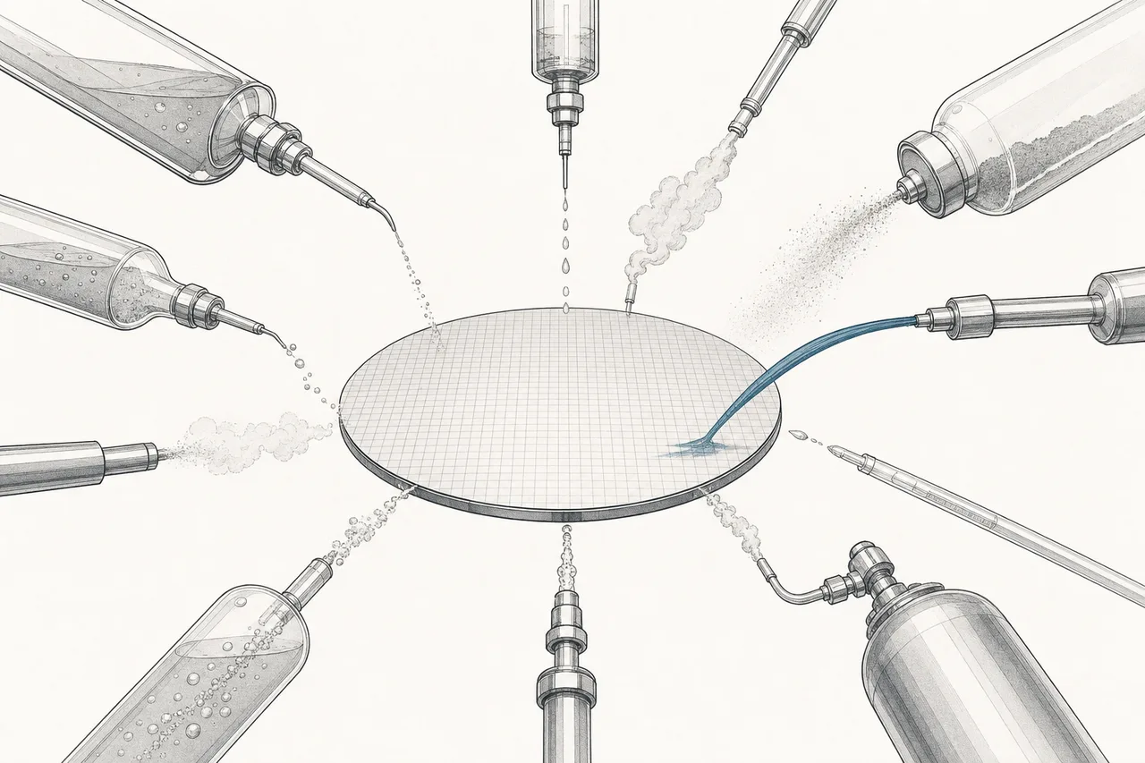
Put simply, Materials & Specialty Chemicals are the 'consumables' a chip plant (fab) uses up in production. Not the equipment you buy once and use for years, but the stuff poured in and consumed with every single wafer. There are four main groups: silicon wafers, photoresist, special gases (electronic gases), and polishing/wet chemicals (CMP slurry and wet chemicals).
The chip industry splits things into two camps · Equipment = what you buy once and use for years, like an EUV machine or an etch tool — that's the Wafer-Fab Equipment field · Consumable / Materials = what gets used up with every wafer and has to be reordered constantly — that's this node. This is why the materials business has 'steadier' revenue than the equipment business: as long as a fab is running, it has to keep buying consumables.
On our megatrend map, this node is a sub-theme of Semiconductors, sitting at the 'upstream' (supply chain) layer — literally the starting point of everything. Because no matter how brilliant a chip's design is, or how advanced the machines are, if there's no pure silicon wafer to start with, nothing can happen at all.
02Why the 'boring stuff' matters at a global level
On the surface it sounds like an ordinary materials-selling business — boring, thin margins. But the reality is the complete opposite. In 2025 the global semiconductor materials market hit a record $73.2 billion (up ~6.8% year over year), split into wafer-fab materials at $45.8 billion and packaging materials at $27.4 billion.
But the total isn't the most important thing. What makes this node 'boring but dangerous' is that it's a hidden bottleneck. If any one material runs short, chip plants worldwide grind to a halt. Even with every EUV machine in place and all the skill in the world, without high-enough-quality photoresist you can't make a single cutting-edge chip. And these materials happen to be concentrated in the hands of just a few makers in a few countries.
And it's a market that's clearly 'concentrated' by region. Taiwan has been the world's biggest consumer of chip materials for 16 years running ($21.7 billion in 2025), followed by China ($15.6 billion) and South Korea ($11.2 billion) — the map of who buys the materials is the map of the world's chip-making bases.
03The materials that flow into a single wafer
The best way to understand this node is to follow 'a single wafer' and what it has to take in before it becomes a finished chip. Each material has to be pure to 99.9999999% or better (nine-nines — only a few parts per billion of impurities allowed), because a single speck of dust can ruin millions of transistors.
1. Silicon wafers — the real starting point is a round disc made of single-crystal silicon (300mm across), polished until it's thousands of times smoother than glass, with surface roughness measured in nanometers. This is the 'paper' every chip is printed onto.
A thin coating liquid that's 'light-sensitive.' Its job is to be the chip's 'photographic film' — when a lithography machine shines light (UV or EUV) through a circuit-pattern template, the exposed parts change chemically, then get washed away to leave the circuit pattern you want. The more advanced the chip (the finer the pattern), the sharper and purer the photoresist has to be. The photoresist for the latest EUV machines can be made by only a handful of companies in the world.
2. Photoresist — as described above, this is the heart of 'printing' the circuit pattern, and the area Japan dominates most decisively (more on that in the next chapter).
Electronic gases = dozens of ultra-pure gases used in the steps that 'etch' and 'deposit' thin films onto the wafer. Some are inert (nitrogen, argon), some are highly corrosive (like hydrogen fluoride) · CMP (Chemical Mechanical Planarization) = the step that 'polishes flat' after each layer is deposited, using a 'slurry' of tiny particles mixed with chemicals to flatten the wafer surface to the atomic level before printing the next layer — modern chips have dozens of layers, so this polishing is repeated dozens of times.
3. Special gases and 4. Polishing/wet chemicals — these two groups are the 'little consumables' a fab uses throughout its 300+ process steps. It sounds minor, but together it adds up to a huge sum. And in 2025, lithography materials (including photoresist) and the CMP group were the two fastest-growing categories (double-digit), because the more advanced the chip, the more printing and polishing steps it needs.
04Why Japan dominates almost all of it
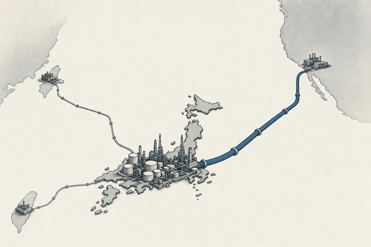
If there's one fact to remember about this node, it's this — Japan controls this materials layer almost completely, even more than it dominates any other layer of the chip industry.
In the silicon-wafer market, two Japanese companies — Shin-Etsu Chemical (~27%) and SUMCO (~24%) — together hold more than half the world. Add the top five (Taiwan's GlobalWafers ~17%, Germany's Siltronic ~12%, Korea's SK Siltron ~9%) and they control ~89% of the 300mm wafer market.
The photoresist market is even more extreme — Japanese companies (led by JSR, Tokyo Ohka Kogyo / TOK, Shin-Etsu, Fujifilm) hold about 80–90% of the global photoresist market. And if you narrow it to photoresist for EUV machines (used to print the most advanced chips), Japan is a near-100% monopoly. JSR alone has over 22% of the photoresist market.
Why is it like this? The answer is that 'purity and quality certification' is a very deep moat. Getting photoresist or gas to nine-nines purity, and then keeping it identical from batch to batch, takes decades of accumulated know-how. And more important — once a fab picks a material and 'qualifies' (certifies) it into its process, switching suppliers means years of re-testing and risks a drop in yield (the share of good chips per wafer). No fab wants to take that gamble, so the incumbents who are already in tend to 'stay for the long haul.'
05How it connects in the ecosystem
This node sits at the 'very bottom' of the chip supply chain, and everything above it depends on it:
- Feeds every sibling field in Semiconductors: whether it's Foundry (TSMC), Memory (DRAM/HBM), or Analog & Power — every plant has to consume this node's wafers, chemicals, and gases every day. No exceptions
- Works in tandem with Equipment: ASML's EUV machine is worthless without photoresist made specifically for EUV — machine and material have to advance as a pair. Every time chips step up one level, both the machine and the resist must upgrade together
- Feeds AI indirectly: this is the hottest relationship right now. The whole AI boom needs more chips = more wafers, chemicals, and gases. Demand flows all the way back down to the deepest materials layer
- Depends in turn on Critical Materials: this node itself depends on materials one layer deeper still — high-grade silicon, rare metals, fluorite (for making HF) — which makes it just as sensitive to global supply-chain tensions
06Where it stands now
2025–2026 is the 'hottest' this node has been in years, for two reasons pulling in opposite directions: the first is the wave of AI demand making everything scarce and pricey, and the second is the geopolitical game that has every country wanting its own materials.
The AI-demand side is very clear. SEMI expects cutting-edge (≤7-nanometer) chip capacity to grow from 850,000 wafers/month in 2024 to 1.4 million wafers/month in 2028 — about 69% growth. And these cutting-edge chips 'eat materials' far more heavily than ordinary chips, because they have more layers and more print-and-polish steps. So the CMP (polishing) group is growing especially fast, around 20% a year through 2028.
The geopolitical side is just as hot. China is racing to make its own materials, after learning that relying on Japan and the US is a weakness — photoresist made domestically in China was only about 10–20% (localization) in 2024, but Beijing aims to push it to 40% by 2026 and 50% by 2027–2030. China even issued its first national standard for EUV photoresist in 2025 to speed up self-reliance.
At the same time, Japan and Korea are investing heavily. Shin-Etsu and SUMCO poured in over ¥150 billion (~$1 billion) in 2025 to add 200,000 wafers/month of high-flatness wafer capacity for 2nm/3nm chips, while TOK and JSR are rushing investment into photoresist for 2nm chips — everyone is racing to expand to ride the AI wave.
07The road ahead
The first direction is clear: AI will keep pushing materials demand for years. And what matters more than volume is 'intensity' — the more advanced the chip, the more materials it eats per wafer, with more layers, more polishing rounds, and higher purity required. So the advanced-photoresist and CMP groups will stay the fastest-growing (double-digit a year) for years to come.
The second direction is diversifying supply for security. After the 2019 lesson (more in the next chapter), every chip-making country wants a domestic materials backup. China is racing to make its own, Korea is investing in domestic HF and chemicals, and the US is pulling materials plants close to new fabs (for example, Entegris building a plant near Intel's Ohio campus) — a chain once centralized in Japan is gradually spreading out. But it's slow and expensive.
The third direction is that materials will be 'tied to the customer' more. As chips get more advanced, chemicals and gases get co-developed with each fab more and more, making the materials maker–customer relationship tighter and harder to switch — which only deepens the incumbents' moat.
08Challenges & risks
This node's appeal — its concentration and deep moat — is also its biggest risk at the same time.
The first and most memorable risk is that materials can become a 'weapon'. In July 2019, Japan announced export controls on three key chemicals to South Korea — photoresist, hydrogen fluoride (HF), and fluorinated polyimide — amid a historical dispute. HF exports to Korea plunged about 88% during that period, instantly disrupting Samsung and SK Hynix (which together make ~72% of the world's DRAM and ~50% of its NAND). The event showed that the most 'boring'-looking thing can be the most powerful geopolitical pressure point.
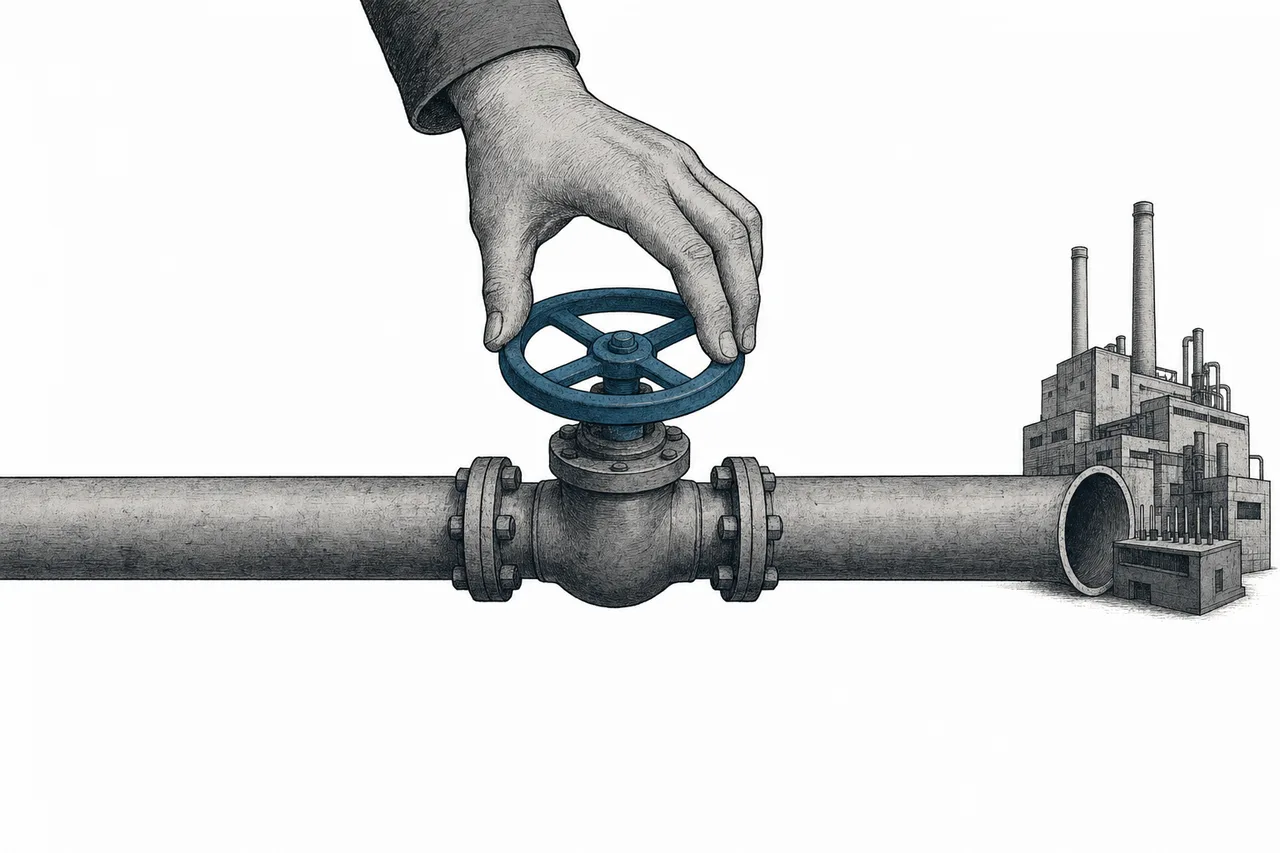
What's interesting is that the long-term side effect cut both ways for Japan itself. After being squeezed, Korea responded by rushing to find new sources (Belgium, the US, Taiwan) and pouring money into domestic materials — SK Hynix invested over ₩320 billion (~$268 million) to qualify domestic materials between 2019 and 2021. The lesson: using materials as a weapon can actually speed up customers 'ending their dependence on you.'
The second risk is China catching up. As China pours everything into making its own materials (a photoresist-localization target of 40% in 2026), over the long term it could press down prices and share for the incumbents in commodity-grade materials (even though the most advanced group, like EUV photoresist, will still be hard for China to catch up to anytime soon).
The third risk is the chip-industry cycle. Because this node is a 'consumable' tied to how much the world's fabs are running, when the chip industry turns down (such as during a memory glut), materials demand shrinks right along with it — and while it swings less than the finished-chip business, it can't escape the cycle either.
In short: this node is the story of the 'boring stuff you can't do without' — silicon wafers, chemicals, and gases that carry no logo on any product you use. But without them, the iPhone, NVIDIA's GPUs, and every electric vehicle couldn't be made at all. To truly understand this layer is to understand why 'boring chemicals' end up on the international negotiating table, no differently from the most advanced chips.