Megatrend · Critical Materials
The shiny round disc every chip on Earth has to start from
Before there's an NVIDIA GPU, before there's the chip in your phone, there always has to be a round, silvery disc first — a single-crystal silicon wafer, pure to “nine nines,” so flat that even light waves stumble on it. This is the “paper” that billions of transistors get built onto. And the whole world buys it from just five companies that together control about 80% of the market. One of them is the Japanese market leader most people have never heard of. This is the story of the quietest base material there is — and one of the deepest bottlenecks in the entire chip industry.
01What it is — the paper of the chip
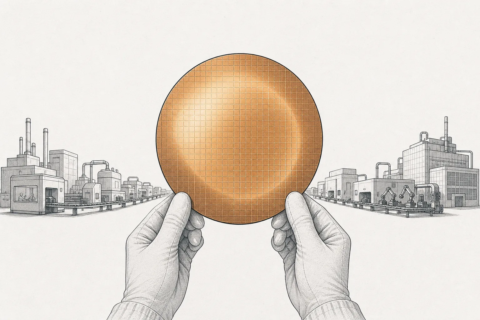
When we look at photos of a chip factory, we usually see people in white suits holding round, silvery discs that reflect light like a mirror. That disc is the wafer — and it's the “paper” that every chip gets drawn onto. Billions of transistors, nano-scale wiring, all of it is built on the surface of this disc. If the disc is bad, it doesn't matter how expensive ASML's lithography machine is — the chip is ruined.
This node is about that silicon disc itself — specifically a disc made of single-crystal silicon that's pure to “nine nines” (99.9999999%) — meaning fewer than one impurity in a billion. The industry's standard size today is 300 millimeters (12 inches). One side is polished so flat that if you scaled the disc up to the size of Thailand, the tallest bump wouldn't reach the height of a single car.
Wafer = the thin, round silicon disc that forms the base of a chip · Substrate = a broader word, meaning the “base material” we build circuits onto (here, the silicon wafer) · Prime wafer = the top grade used for making real chips (different from a test wafer) · Epitaxial (epi) wafer = a wafer with an extra ultra-thin crystal layer grown on its surface, to reach the highest quality for advanced logic chips — pricier, and in high demand in the AI era.
On the megatrend map, this node is a branch of Semiconductor Materials under the larger trend Critical Materials & Supply Chain. It sits alongside three siblings: chemicals and photoresists (the chemicals used to print patterns), specialty gases, and compound semiconductors (GaN/SiC/GaAs) (special base discs that aren't silicon). We focus on the silicon disc, the most widely used base, and we look at it through a “critical materials” lens — not just who sells the most, but “if it runs short, who's in trouble.”
02Why it matters — the industry's silent bottleneck
What makes wafers interesting isn't the size of the market — it's the concentration. The world's silicon wafer market in 2025 is worth about $14.5 billion — tiny next to the total chip market of over half a trillion dollars. But every chip on Earth has to start from this disc. If the discs run short, no factory can make anything at all — that's the perfect definition of a “bottleneck.”
And this bottleneck really is narrow. The whole world buys wafers from just five companies that together control about 80% of the market, led by Shin-Etsu Chemical (Japan, ~28%) and SUMCO (Japan, ~23%). These two alone make up more than half of the world's 300mm wafer capacity. They're followed by GlobalWafers (Taiwan), Siltronic (Germany), and SK Siltron (South Korea).
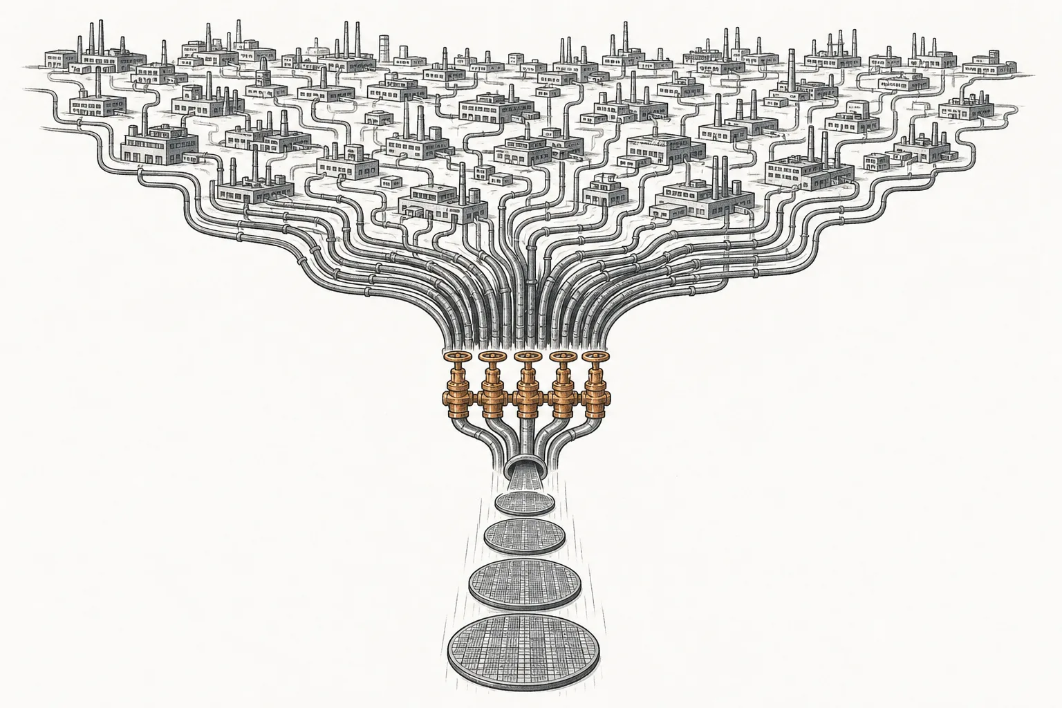
Why only five? Because the barriers are enormous. Making silicon crystal pure to nine nines and flat at the atomic level, on a large 300mm disc that has to be uniform across each disc and from disc to disc, is a skill built up over decades. A single plant costs billions of dollars to build, and it's a thin-margin business that swings with the cycle — so new entrants find it hard to break in. That's why this “ordinary-looking round disc” has become a strategic point that the US, Europe, and China all want to have for themselves.
03How it works (from sand to a 300mm disc)
Turning “sand” into a silicon disc ready for the chip factory is a long, painstaking process. Let's walk through, step by step, how a single shiny round disc comes to be — the heart of it all is a middle step called Czochralski.
The heart is step 3, the Czochralski method (pronounced “cho-KRAL-ski”) — put pure polysilicon in a quartz crucible, melt it at about 1,420°C into a red-hot liquid, then dip a tiny “seed crystal” to touch the surface. From there you slowly pull it up while rotating, and the silicon atoms line up along that seed to become a single, seamless crystal. Keep pulling and you get a cylindrical ingot about 300mm across and over a meter and a half long. Controlling the pull speed, temperature, and rotation just right is the hardest art to copy.
That ingot then gets sliced into thin discs with a diamond wire, then polished with CMP (Chemical Mechanical Polishing) — using a chemical slurry to make the surface smooth and shiny at the atomic level. Finally, the top-grade discs get an ultra-thin crystal layer grown on the surface (epitaxy) for the best quality for advanced chips — and out comes a 300mm disc, ready to ship to the chip factory, where hundreds of rounds of deposit–and–etch will begin.
04Where it sits in the ecosystem
If you picture the whole chip industry as a river, the wafer is the very top of the materials stream — it's the first thing to flow into the factory, and everything after is built on top of it. So this node is inseparably linked to its neighbors:
- Feeds directly into chip factories (Foundry & Contract Fabrication): TSMC, Samsung, and Intel buy blank discs from these five and then “carve” chips onto their surface — no disc, nothing to carve. The more chip factories get built, the more discs get bought
- One of the “materials” in Semiconductor Materials & Specialty Chemicals: from the angle of the chip materials business, the wafer is the biggest and best-known product — this node is the “critical materials” lens on the same thing, focused on supply fragility, not just sales
- Paired with chemicals and photoresists: a blank disc has to be coated with photoresist before any pattern can be printed, and CMP needs its own polishing slurry — wafers and chemicals move together the whole way
- Different from compound semiconductors (GaN/SiC): a silicon wafer is the “main base disc” for ordinary digital chips, while GaN/SiC discs are special base discs for high-power, high-frequency chips — different material, different market, but relatives in the same group
- Demand is pulled by AI and Cloud & Digital Infrastructure: the AI chips and HBM memory that data centers fight to buy need more and more high-quality epi discs — the AI wave flows all the way back down to this base-material layer
05Where it stands now
After the slump from the 2023–2024 inventory glut, the wafer market clearly recovered in 2025. According to SEMI's report, total wafer shipments for 2025 rose 5.8% to 12,973 million square inches — and more importantly, first-quarter 2026 shipments jumped 13.1% year over year. The engine pulling it is AI directly — both epi discs for advanced logic chips and polished discs for HBM memory.
The market leader is still Japan's Shin-Etsu Chemical — an old chemical company whose wafer division (Shin-Etsu Handotai) has long been number one in the world. It's followed by fellow Japanese maker SUMCO. The two are now jointly investing about $1 billion (¥150 billion) to add roughly 200,000 wafers/month of extra-flat capacity, to support 2- and 3-nanometer chips, while SUMCO has announced it will stop making 200mm wafers at its Miyazaki plant by the end of 2026 to pour everything into AI-grade 300mm discs.
The biggest tremors come from two directions. The first is spreading production out of Asia — Taiwan's GlobalWafers opened a $3.5 billion 300mm wafer plant in Sherman, Texas in May 2025 (the first new wafer plant in the US in 20 years), and announced another $4 billion in investment, for a total plan of about $7.5 billion — to give the West its own “backup tap.”
The second is China's rise. Under pressure to become self-reliant, Chinese makers are racing to build 300mm discs at home, led by National Silicon Industry Group (NSIG), Shanghai Silicon Industry, and TCL Zhonghuan. Together these three account for about 35% of prime 300mm wafer shipments in the China market, and they keep expanding — TCL Zhonghuan signed a five-year deal to supply Hua Hong with roughly 300,000 12-inch wafers/month starting mid-2026, while NSIG got the green light to build a new $1.2 billion plant in Chongqing.
06The road ahead
The first direction is “300mm is everything” becoming ever clearer. The 300mm disc already holds about 75% of the market by value, and it will grow further as all advanced chips move to this size. Makers are shutting down old 200mm wafer lines one by one to pour capacity into high-grade 300mm, especially the epitaxial discs in high demand for AI chips — a steady shift of value from “ordinary discs” to “premium discs.”
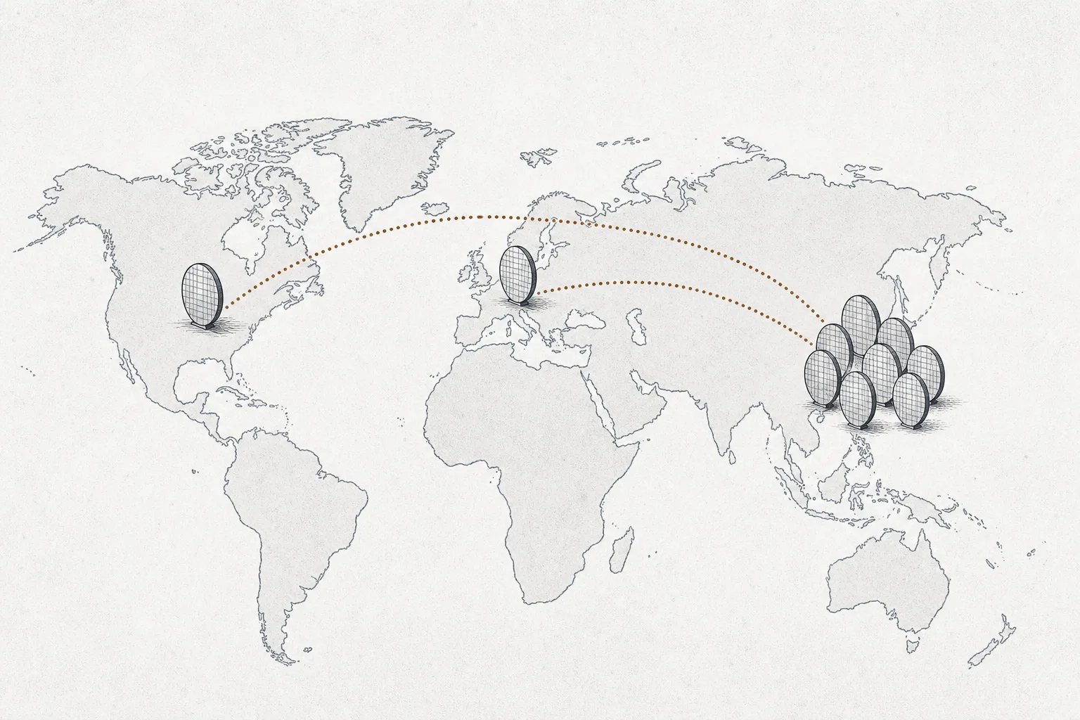
The second direction is geographic risk diversification. The lessons of COVID and US–China–Taiwan tensions made everyone reluctant to depend on a single source. So the US and Europe are pulling wafer plants closer to home (like GlobalWafers in Texas, Siltronic in Singapore), while China builds a parallel domestic chain — the wafer world is slowly splitting into several more self-reliant regions.
The third direction is demand growing by “silicon area,” not just chip count. An AI chip is much bigger than an ordinary chip, and it usually comes paired with multi-layer HBM memory. So each GPU “eats” more wafer area than before — wafer demand grows faster than the number of chips sold. It's a structural tailwind tied directly to the worldwide expansion of AI data centers.
07Challenges & risks
The first risk is severe cyclicality. The wafer business is tied to chip factories' investment cycles and to customers' inventory levels. When the industry is booming, orders overflow and prices are good. But when the cycle flips, customers stop ordering to clear inventory, and revenue can shrink for years — exactly what happened in 2023–2024, when shipments contracted before recovering in 2025. It's a thin-margin business that has to weather high volatility.
The second risk is concentration as a double-edged sword. Having only five companies gives the leaders bargaining power, but it also means the whole world is fragile to a single-point event — an earthquake in Japan (where Shin-Etsu and SUMCO are concentrated), a factory fire, or trouble at any one maker could shake supply across the whole chain. And because Japan's 300mm discs hold more than half the world, the geographic risk is higher than many people think.
The third risk is China's catch-up and a price war. State-subsidized Chinese makers are aggressively ramping up 300mm capacity. Short term, that's a new chunk of demand (China buying / building at home), but long term, if China overproduces beyond domestic need, it could push global wafer prices down — as happened before with solar panels and energy silicon wafers. Over the long run, it's a threat to the margins of the existing five.
In short: this node is the quietest shiny round disc in the chip supply chain — no one sees it in the GPU or phone they're using, but everything starts from it, made by just five companies that together control nearly the whole world. To understand this layer fully is to understand why the “paper of the chip” is one of the deepest and most fragile bottlenecks of the AI era.