Megatrend · Critical Materials
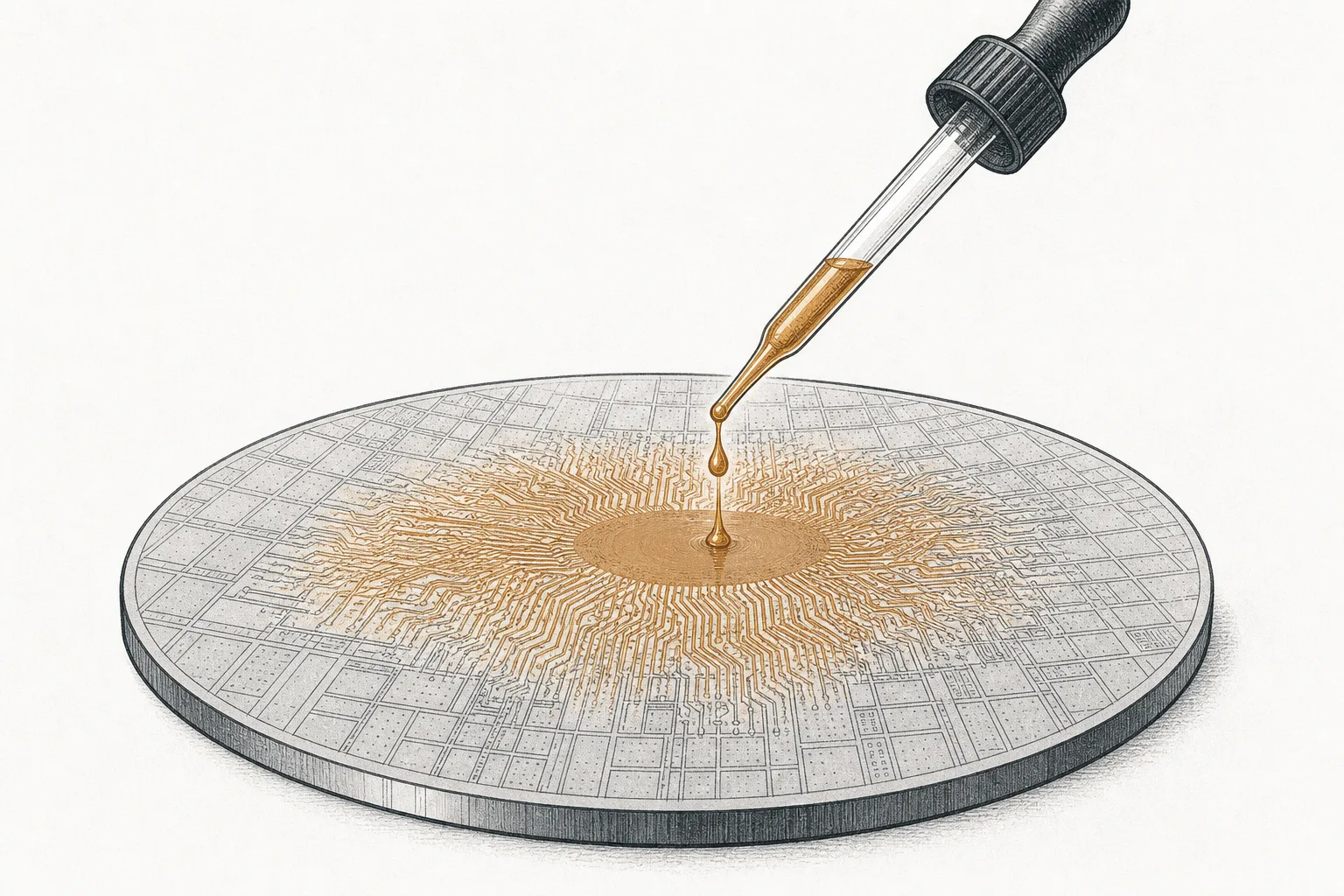
A single drop of light-sensitive liquid — the stuff that "draws" the circuits onto every chip in the world
ASML's lithography machines, costing billions per unit, usually get the credit as the hero that prints a chip's patterns. But the thing that actually "receives the light" and becomes the circuit pattern is photoresist — a wafer-thin light-sensitive chemical coated onto the wafer. It comes with a family of siblings: polishing liquid (CMP slurry), etchants, and ultra-pure cleaning chemicals. The market is small, but Japan owns almost all of it — and EUV resist for the most advanced chips is one of the narrowest bottlenecks in the entire industry. This is the story of the "chemistry" that decides how fine a chip can get.
01What it is
Think of printing a circuit onto a chip like developing a photo back in the film days — you have "light" shining through a negative, but without light-sensitive photo paper to receive it, that light means nothing. In the world of chips, that photo paper is photoresist — a wafer-thin chemical that changes its properties when light hits it. And it's what makes nanometer-scale circuit patterns actually "stick" onto the wafer.
This node is the whole group of process chemicals used to build and clean chips — not the machines, but the "inks and liquids" those machines use. It breaks into four main groups: (1) photoresist, the light-sensitive liquid that creates the circuit pattern — the star, and the hardest · (2) CMP slurry, the liquid that polishes the wafer surface flat to the atomic level before building the next layer · (3) etchant, the acids and chemicals that carve material away along the pattern · (4) cleaning / wet chemicals, which wash away residue to a level where a single speck of dust can ruin a chip.
Photoresist = a light-sensitive polymer coated onto the wafer. When light hits it following the pattern of a mask, the exposed part either "becomes easier to dissolve" (positive resist) or "hardens" (negative resist) when you wash it · It must be matched to the wavelength of the light — resist for DUV light (193 nm) won't work for EUV (13.5 nm); you have to redesign the whole formula · CMP (Chemical-Mechanical Planarization) = polishing the wafer surface perfectly flat using a liquid that contains both chemicals and tiny abrasive particles, before building the next circuit layer on top.
On the megatrend map, this node is a sub-branch of Semiconductor Materials under the larger trend Critical Materials & Supply Chain. It sits alongside the silicon wafer (the base material these chemicals work on), specialty gases (their partner in the etch and deposition chambers), and compound semiconductors (GaN/SiC) — if the wafer is the "paper," this node is the "ink and cleaning fluid" you can't do without on any page.
02Why it matters — one island controls the world's liquids
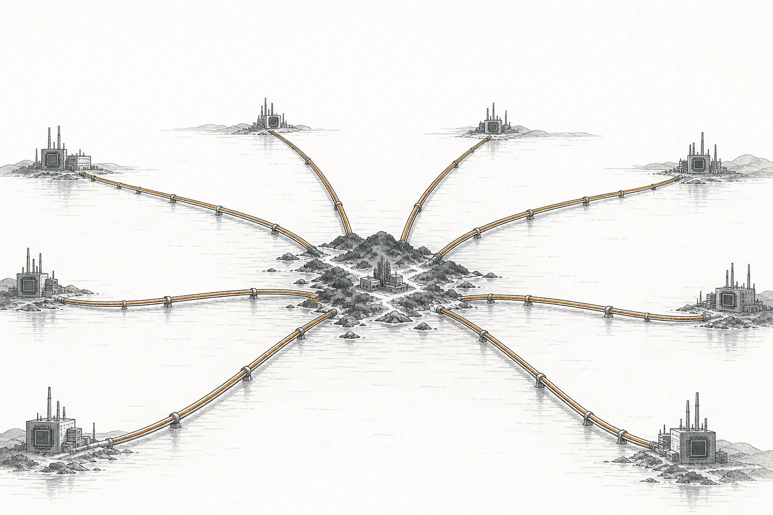
What makes this node special isn't the size of the market, it's the concentration in a single country. The global photoresist market in 2025 was worth about $6.7 billion — tiny next to the $600 billion chip market. But a handful of Japanese companies control roughly 75–90% of the market, and at the most advanced tier — EUV resist — the number gets even more startling: Japan controls more than 95%.
The world learned this lesson the hard way in 2019, when Japan restricted exports of three chip chemicals to South Korea — photoresist, hydrogen fluoride (HF), and fluorinated polyimide. At the time Korea depended on Japan for 93.2% of its photoresist, and Samsung and SK hynix had to scramble almost overnight for backup sources from Belgium and elsewhere. That event woke the whole world up to the fact that "a tiny liquid nobody talks about" can genuinely shut down chip factories worth hundreds of billions.
Why does Japan dominate this much? The answer is purity and know-how accumulated over decades. Photoresist isn't just "colored liquid" — it's a polymer whose purity has to be controlled down to parts per billion (ppb), because even a trace of a foreign particle can ruin a transistor. Tuning the formula for each new chip generation takes years of working alongside the chip factory — and that's the wall that makes it enormously hard for newcomers to cross, and why this market stays concentrated among the same incumbents.
03How it works (coat–expose–wash–etch)
The heart of this node is turning "light" into a "pattern you can touch" on the wafer, through light-sensitive liquid. Let's walk through, step by step, how a single layer of circuit pattern comes to be.
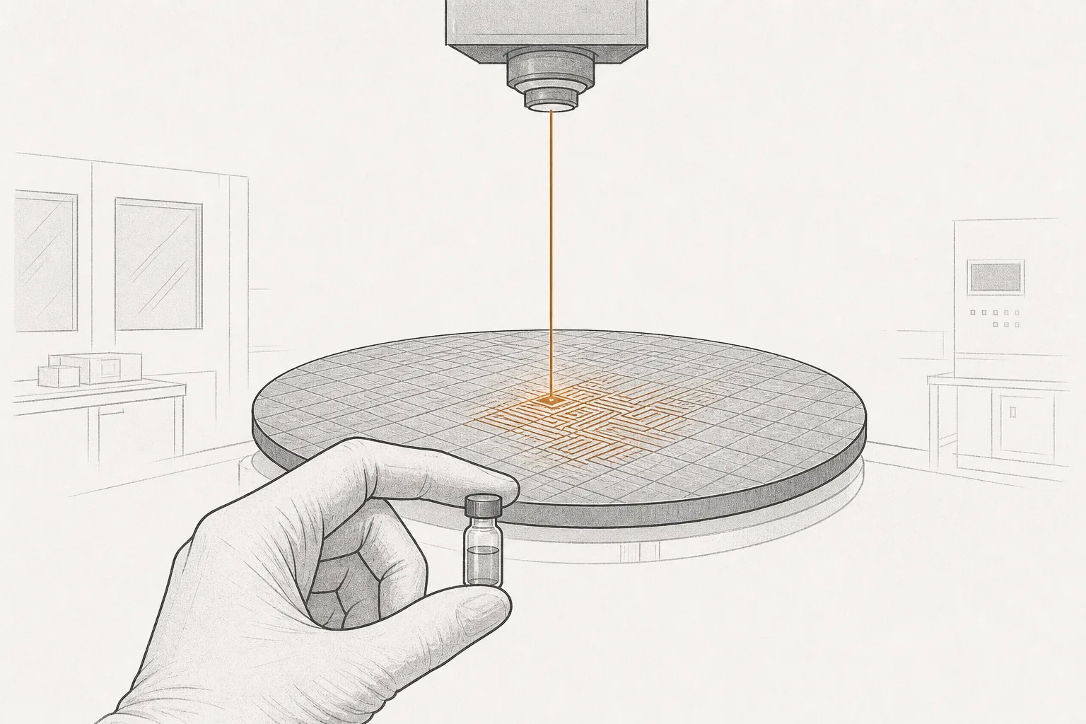
What makes this group of chemicals "hard" is that every step has to be precise down to the nanometer — the liquid must be coated thin and evenly across the whole wafer, sensitive to light just right (too sensitive and it blurs, not enough and it won't stick), and clean enough to have almost no impurities. The toughest of all is EUV resist, because EUV light at a wavelength of 13.5 nm carries high energy and very few photons per point, creating a "randomness" (stochastic effect) that makes circuit lines uneven — the resist has to be designed to absorb EUV light well and keep this randomness under control, which is the hardest chemistry problem in 20 years.
The other liquids work right alongside it: CMP slurry polishes the surface perfectly flat before building the next layer (if the surface isn't flat, the light can't focus) · etchant works with the resist in the fourth step · and cleaning liquid washes away residue between every step — in a single chip with over a hundred layers, this cycle repeats hundreds of times, using this entire group of chemicals each time.
04Where it sits in the chip industry
Process chemicals are the "consumable" a chip factory has to keep refilling all the time — unlike machines you buy once and use for years, these liquids get used up with every wafer. So they're tightly woven into every node around them:
- The "consumable" of Wafer-Fab Equipment & Lithography: ASML's lithography machines, costing billions apiece, are "worthless" without the resist matched to their light — the machine fires the light, but the resist is what receives it and becomes the pattern. The two must always advance together. And the etch/deposition machines in the Deposition & Etch group consume this node's etchants and cleaning liquids at every step
- The "raw material" of Semiconductor Materials & Specialty Chemicals: seen from the angle of Semiconductors, this group of chemicals is one of the materials fed into the factory — this lesson looks through the critical-materials lens, meaning "who controls the supply," while the lens of the manufacturers' business lives at node 56070000
- Works on the silicon wafer and pairs with specialty gases: the wafer is the "canvas" these liquids draw their patterns on, and in the etch and deposition chambers, the liquids and specialty gases work as a pair — these three are siblings in the same Semiconductor Materials family
- Demand flows back from AI and Cloud & Digital Infrastructure: the more complex an AI chip and the more layers it has, the more coat–expose–etch cycles per chip = more liquid used per wafer. So this node's demand grows with the "complexity of the chip," not just the number of chips
05Where it stands now
The event that tells you everything about this era happened in 2024 — the Japanese government, through its fund JIC (Japan Investment Corporation), acquired JSR, the world's largest photoresist maker, for about $6.4 billion, then delisted it from the Tokyo Stock Exchange in June 2024. The state didn't buy a chip company or machinery — it bought a liquid maker — a clear sign that photoresist is now seen as a "strategic national asset" on the same level as military materials.
The competitive picture right now is highly concentrated: Tokyo Ohka Kogyo (TOK) leads with about 30% share in 2024, followed by JSR at around 27%. And the top five advanced-resist makers combined (JSR, TOK, Fujifilm, Shin-Etsu, Dongjin Semichem) take about half of all advanced resist. The hottest market is EUV resist, growing from about $226 million in 2024 to nearly $880 million in 2030 — over 25% a year — and only TOK, JSR, and Shin-Etsu have passed the standard to supply real production lines.
Companies are racing to invest ahead of demand for 2 nm chips: Fujifilm launched a negative-tone EUV resist along with a cleaning liquid in October 2024, and in June 2025 expanded its Kumamoto plant to raise EUV resist capacity by 30% to fill orders from TSMC · Shin-Etsu announced an investment of about $500 million to build a new lithography-materials plant, with the first phase finishing in 2026 · and in September 2025 Lam Research cross-licensed patents with JSR/Inpria to accelerate metal-oxide and dry-resist EUV — resist technology seen as the next game-changer.
Another pillar that isn't in the news but matters just as much is CMP slurry, a market of about $3.1 billion in 2025, growing to $4.3 billion by 2030. Here the West can still compete — Entegris (after merging with CMC Materials) holds about 22–25% share and has a deal to supply slurry to TSMC, while Japan's Resonac is another leader. Asia-Pacific combined controls about 82% of the CMP market, reflecting how the center of process chemicals sits close to the chip factories in Asia.
06The road ahead — the EUV resist era
The first direction is EUV resist becoming the main battlefield. As chips push toward 2 nm and below, printing the patterns depends more and more on EUV, and the resist matched to it is an indispensable piece. The competition is shifting from the old chemically amplified resist toward metal-oxide resist (like the tin-oxide technology from Inpria, which JSR bought), which absorbs EUV light better and controls the randomness of circuit lines more precisely — seen as the biggest shift in resist technology in 20 years.
The second direction is ever-rising purity. The smaller the circuit gets, the more an impurity that was once "acceptable" becomes a problem — makers have to drive contaminants down further from the ppb level and shrink the particle sizes in the liquid. This opens room for players strong in "extreme cleanliness" (in cleaning liquids and slurry, say) to grow, even without competing head-on with the resist leaders.
The third direction is diversifying away from Japan. After the lessons of 2019 and 2024, Korea, Taiwan, the U.S., and Europe are all trying to build their own sources of resist and process chemicals — Korea is backing Dongjin Semichem, the U.S. has DuPont and Entegris, and Europe has Merck (EMD Electronics). But the reality is slow and hard, because the know-how barrier is high. Dependence on Japan will gradually ease, but it'll take a decade, not a year or two.
07Challenges & risks
The first and most prominent risk is concentration in Japan. When almost all of the world's EUV resist comes from just three Japanese makers, the fragility is very high — a natural disaster (Japan is an earthquake zone), a factory accident, or a single problem in the chain could shake the whole chip industry. And because tuning a resist formula for a new factory takes years of testing, finding a backup source on short notice is nearly impossible.
The second risk is being used as a trade and geopolitical weapon. 2019 proved that chip chemicals can genuinely be a bargaining chip. Just announcing export controls sends prices soaring and stalls production lines. In a world where U.S.–China–East Asia tensions are still high, this group of chemicals is a point where you can "dial down the tap" — and everyone knows it. That's exactly why the Japanese government itself acquired JSR, to keep this card in hand.
The third risk is the boom-and-bust cycle of the chip industry. Even though the liquids are a consumable that sells continuously, the volume used is tied to how fully the chip factories are running. When the chip industry slows, demand for the liquids falls with it, and big investments to expand EUV resist capacity are risky if the timing of a technology shift (say, metal-oxide vs dry resist) doesn't go as expected — betting on the wrong technology means losing both the investment and the time.
In short: this node is the wafer-thin chemistry that genuinely "draws" the circuits onto every chip — photoresist that receives the light and becomes the pattern, along with the polishing, etching, and cleaning liquids that finish every layer. It's one of the quietest yet most powerful bottlenecks in the chip economy — and the finer chips get, the more important the role of "the chemistry that draws the pattern" becomes.