Megatrend · Critical Materials
A crystal that takes weeks to grow — and it's the bottleneck for every EV on the planet
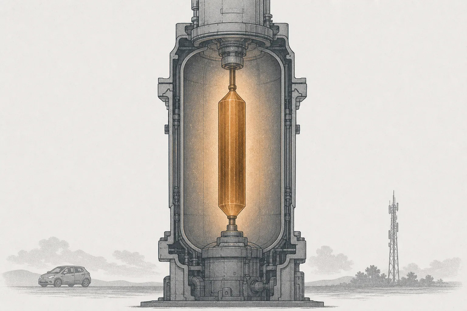
Almost every chip we use is made of "silicon." But some of the heavy lifting — the high voltage in an EV inverter, fast charging, 5G signals, the lasers in an AI data center — is something silicon does poorly. For that you need a different family of crystals: compound semiconductors (silicon carbide SiC, gallium nitride GaN, gallium arsenide GaAs, indium phosphide InP). Here's the secret: the hardest, most valuable step isn't making the chip — it's growing the crystal in the first place. SiC has to be grown in a 2,500°C furnace for weeks just to yield an ingot a few centimeters long. This is the story of a tiny raw material that decides the whole game.
01What it is — the crystal base that isn't silicon
Almost every chip in the world starts as a thin round disc called a wafer, and most are made of silicon — an element that's easy to find, easy to grow into a crystal, and cheap. We told that story in Silicon Wafers & Substrates. But this lesson is about "the other family" that silicon can't stand in for — compound semiconductors, made by combining two or more elements into a crystal.
There are four leads worth knowing, each good at a different thing:
- SiC (silicon carbide): handles high voltage and heat far better than silicon → the heart of EV inverters, fast chargers, and solar/industrial power systems
- GaN (gallium nitride): switches on and off very fast with low energy loss → tiny fast-charging adapters, 5G signal amplifiers, radar
- GaAs (gallium arsenide): strong at high frequencies and light → RF chips in phones, lasers, sensors
- InP (indium phosphide): sends light signals the fastest → lasers and transceivers in fiber optics and AI data centers
But the core of this node isn't the "chip" itself — it's the substrate, the "base plate" of starting crystal. Before there's an SiC chip for an EV, there has to be an SiC ingot, which is then sliced into base plates. And this step of "growing the ingot" is the hardest, scarcest, most valuable part of the entire chain.
Substrate = the crystal base plate used as the "floor" to build the chip on top of · Wide-bandgap = the property that lets SiC/GaN "withstand" higher voltage and heat than silicon, which is why they suit high-power work · Boule (ingot) = the cylindrical single-crystal block that's grown, before it's sliced into wafers
On the megatrend map, this node is a leaf of Semiconductor Materials in the Critical Materials & Supply Chain family, with siblings Silicon Wafers (ordinary silicon wafers), Process Chemicals & Photoresist, and Electronic & Specialty Gases — we focus only on "the crystal base plates that aren't silicon."
02Why it matters — and why "growing the crystal" is the bottleneck
Why does the whole industry put up with a material that's dozens of times harder to grow than silicon? One word: efficiency. An EV with an SiC inverter goes farther on the same battery, because SiC loses less energy as heat. Fast chargers and 5G base stations get smaller and run cooler thanks to GaN. And AI data centers, which shuttle huge amounts of data between chips, rely on InP lasers that are far faster than copper — the most "important and power-hungry" jobs of this era all run on these compound materials.
The market reflects this clearly. The total market for compound-semiconductor substrates and epi-wafers is expected to top $5 billion by 2031, growing at roughly 14% a year. N-type SiC alone is projected to pass $2 billion. And InP is the fastest-growing dark horse — over 18% a year, riding the AI wave.
But why is the "base plate" the bottleneck, not the chip itself? The answer is in growing the crystal. Silicon is grown with the Czochralski method — dip a seed crystal into molten silicon and slowly pull it up. It can grow as fast as ~10–14 centimeters an hour. But SiC can't be melted the normal way. So you use PVT (physical vapor transport) — heat SiC powder until it sublimes into vapor at about 2,100–2,500°C, then let that vapor settle onto a seed crystal bit by bit. It grows at just ~0.3–0.8 millimeters an hour.
This is why the value concentrates "upstream" — a process that's scorching, slow, opaque inside, and full of points where the crystal can fail (tiny holes called micropipes, dislocations). That makes yield low and the deep know-how hard to copy. Whoever can grow large, clean crystals first controls the game — while actually turning the base plate into a chip is the job of the device-side node that comes after (EV Power Semiconductors).
03How it works (from ingot to chip)
The road from "powder" to "chip" has four big steps, and almost all the value and difficulty is packed into the very first one. Let's walk through them one at a time.
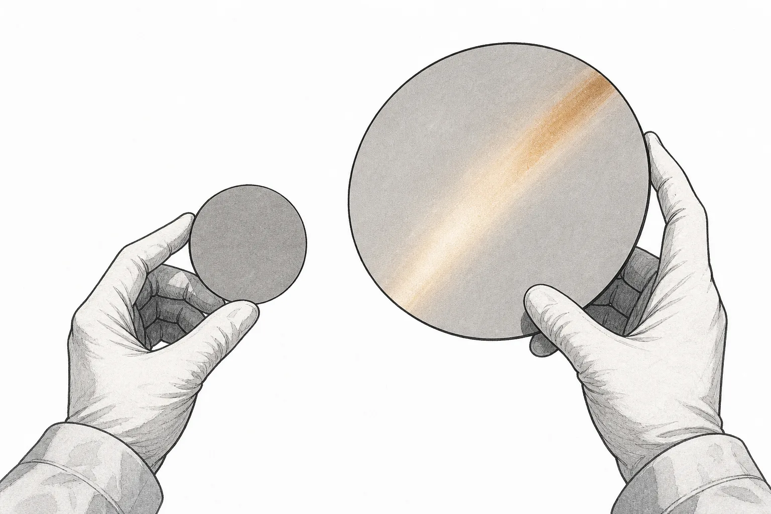
Why is the first step so "expensive"? Because it's invisible and can't be fixed after the fact — while growing, the crystal can develop micropipes (tiny holes that run all the way through the ingot) or dislocations that ruin the chip on top. Once you slice it into plates, wherever there's a defect, that spot is unusable. The bigger the plate (from 6-inch to 8-inch), the harder it is to control — but a bigger plate is far more worth it because you cut more chips per plate. That's why "going to 8-inch" has become the industry's main battleground.
04Where it sits in the chip world
This node is the "upstream raw-material layer" of the chip world — it supplies the base plates that others build on. Let's see who it connects to.
- Supplies EV Power Semiconductors directly: this is SiC's biggest customer — the power MOSFET chips inside EV inverters and chargers are built on the SiC base plates from this node. To be clear: this is the base-plate material, while designing and making the high-power chip itself is that node's job
- Paired with Silicon Wafers as an alternative: silicon still owns most of the world's chips (cheap and easy to grow), while compound materials are the "complement" for specific jobs silicon does poorly — the two divide the work, they don't fully replace each other
- A raw material for the connectivity side of Logic, Compute & Connectivity Processors: InP/GaAs lasers and transceivers are what move signals fast between chips and through fiber optics — the backbone of data-center connectivity
- Driven by AI, Electrification & Mobility, and Cloud & Digital Infrastructure: these three waves are the end demand — AI drives InP, EVs drive SiC, fast charging/5G drives GaN. The demand flows all the way down to this raw-material layer
05Where it stands now
2024–2025 was a "painful" stretch for the SiC side, even though long-term demand is still strong. Global N-type SiC substrate revenue fell 9% in 2024 to about $1.04 billion. The cause: EV and industrial demand slowed while capacity had been expanded ahead of time, tipping into oversupply. The price of 6-inch base plates dropped more than 60% in 2024, and 8-inch plates plunged from about $1,500 to about $1,000 by early 2025.
The competitive picture is shifting fast. The old champion Wolfspeed is still number one with about 33.7% share, but it's badly hurt — its stock fell more than 60% in a single year as EV demand slowed, and it's entering a restructuring/cost-cutting phase in 2025 while rushing to shift to 8-inch production lines. Meanwhile Chinese players like TanKeBlue and SICC have surged to number two and three, together passing 34%, with SICC leading on 8-inch plates, while Coherent (which absorbed the former II-VI) has slipped to fourth.
On the exact opposite side from SiC is InP — where demand is exploding on the AI wave. Data centers want InP lasers for high-speed data transmission. AXT of the U.S., which controls 60–70% of the world's InP substrate production, raised capital in late 2025 to expand capacity ahead of a looming shortage. Japan's JX Advanced Metals also announced it would raise InP capacity about 20% — InP is the "bright side" of this node at a moment when SiC is hurting.
06What's next — 8-inch, China, and falling prices
The first direction is going to 8-inch (200mm), the new inflection point on the SiC side. Bigger plates mean more chips and a lower cost per chip. Whoever can grow clean 8-inch crystals in volume first gains an immediate cost advantage — Wolfspeed is betting the whole company on 8-inch production lines (now running at only about 25% utilization while it ramps up), while China's SICC also claims to lead on 8-inch plates. This is a race over "who can control cost first."
The second direction is the rise of China. Under a self-sufficiency policy, China has poured investment into building massive SiC capacity, and Chinese players (TanKeBlue, SICC, and others) together already take more than a third of SiC substrate share — becoming the main force pushing prices down. For buyers (EV makers) that's good news, things get cheaper. But for the old Western champions, it's heavy pressure.
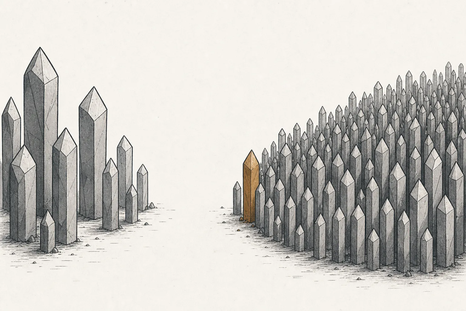
The third direction is InP becoming the star. While SiC faces a price war, InP demand from AI data centers is growing the fastest (over 18% a year) — because optical connectivity has become AI's new bottleneck. Those who already control InP substrate (AXT, JX, Coherent, Sumitomo) are well positioned this cycle. The lesson: within the same node, different materials can sit in completely different phases of the cycle.
07Challenges & risks
The first and hottest risk is oversupply and a price war. Wolfspeed's story is the living lesson — the company expanded capacity ahead of the EV wave, but when EV demand slowed and China dumped cheap product, prices fell hard instead, forcing a company-wide restructuring. A material business that invests heavily ahead of demand "hurts" a lot when the timing of supply and demand doesn't line up.
The second risk is Chinese dumping. When China builds capacity beyond its own demand and accelerates low-priced exports to grab share, higher-cost Western producers get squeezed on profit — just as happened with solar panels and LEDs. This risk isn't just about price; it's about losing long-term share to a state-backed rival.
The third risk is end demand tied to EVs and the cycle. Nearly half of SiC demand comes from EVs. If global EV sales grow slower than expected (shrinking subsidies, high interest rates), demand for SiC base plates stumbles too — a business with a bright long-term future but short-term swings tied to the economic cycle and auto policy.
In short: this node is the crystal that has to be grown in a scorching furnace for weeks, so EVs can drive farther, chargers can get smaller, and AI can move data faster. It's the most deeply hidden bottleneck of the energy transition and the AI era — and it's now entering a phase where prices swing, China rises, and 8-inch technology decides who survives.