Megatrend · Semiconductors
Every chip is built one layer at a time — by "spraying" then "etching," repeated hundreds of times
Lithography — the machine that prints a chip's pattern — usually gets credited as the hero. But the machines that actually "build" the transistors are a different group, working quietly in the background: they spray on films just atoms thick (deposition), then etch away the excess to leave a pattern (etch). Repeat that over a hundred times and you get a single chip. This tool market runs into the tens of billions of dollars a year, is controlled by just a handful of companies, and is the real "picks and shovels" that every AI chip has to pass through.
01What it is
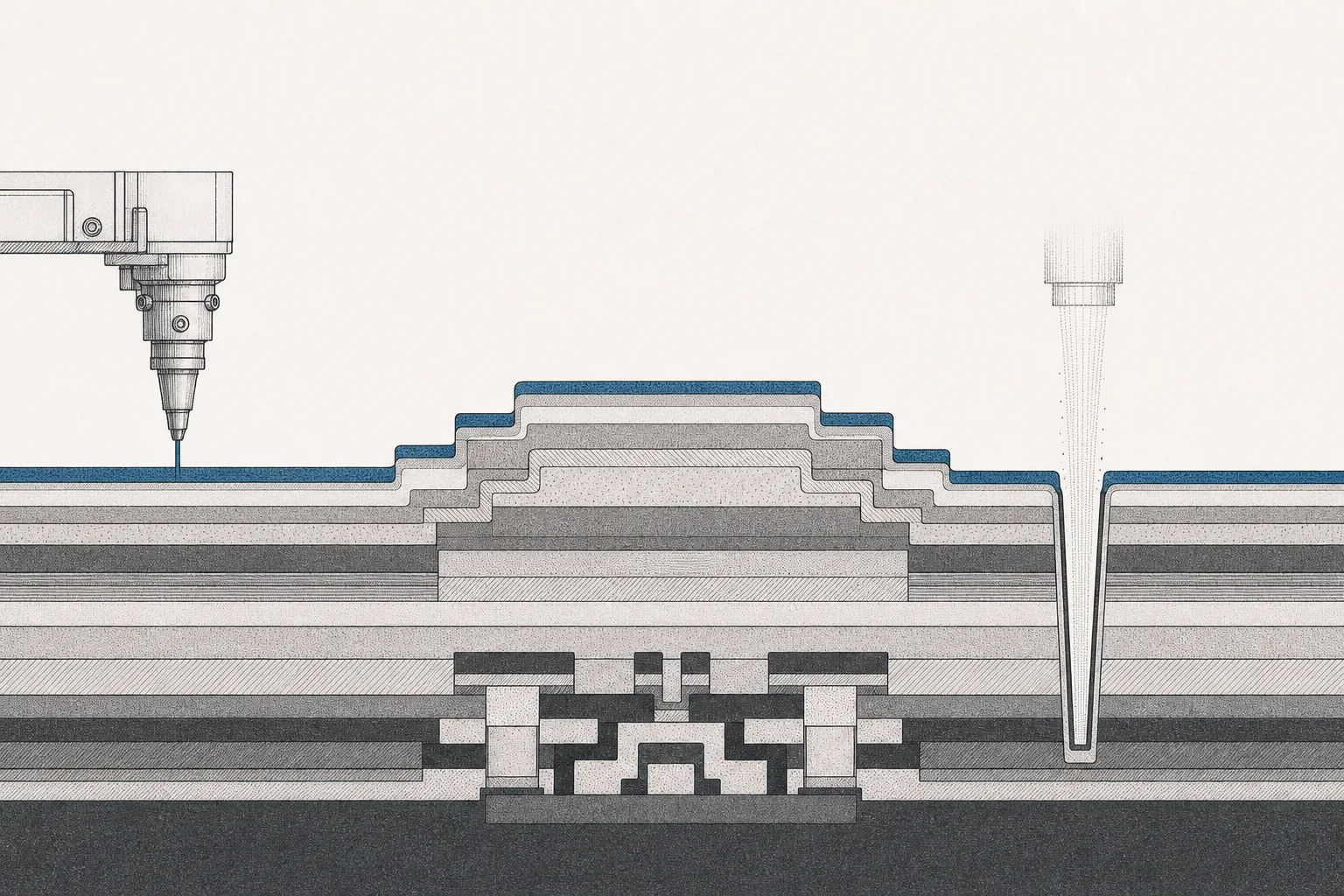
Picture a modern chip not as a flat board but as a tiny hundred-story skyscraper stacked on a slice of silicon. Each floor holds a pattern of wires and switches ten thousand times finer than a human hair. The question is — how do you "build" something that small? The answer isn't to print it all at once. It's to repeat two basic moves hundreds of times: add one layer of material, then etch away the part you don't want.
This is the heart of the node — the group of machines that "add" and "etch," plus two supporting jobs, making four main steps in all: (1) Deposition coats a thin film onto the wafer · (2) Etch removes material along the pattern · (3) Clean washes away residue between steps down to atomic cleanliness · (4) Ion implant fires ions in to change the electrical properties of the silicon. These machines are the hands that actually "carve" the transistors.
On the megatrend map, this node is a branch under Wafer-Fab Equipment & Lithography within the big trend Semiconductors. It sits in the "deepest layer of the supply chain" — the maker of the tools that chip factories then use. Its siblings next door are Lithography Systems (the pattern-printing machines ASML dominates) and Process Control — Metrology & Inspection (the measurement and defect-finding machines). If lithography is the "projector of the blueprint," this node is the "construction crew" that actually builds to that blueprint.
Deposition = coating a thin film onto the wafer (for example, CVD coats via a chemical reaction from vapor, PVD coats by evaporating metal) · Etch = removing material, mostly using "plasma" to dry-etch, for deep and sharp trenches · ALD/ALE (Atomic Layer Deposition/Etch) = the most precise kind — adding or etching one atomic layer at a time, used when you need nanoscale precision in the newest chips.
02Why it matters — the picks and shovels of the AI age
There's a line that fits this industry well: in a gold rush, the ones who get rich for sure aren't the miners — they're the people selling picks and shovels. Whether the AI-chip war ends up won by NVIDIA, AMD, or some tech giant's custom chip, every one of them is made in a factory that has to buy these deposition and etch machines first. This node is the layer that sells shovels to everyone on the field.
The size of the market makes that clear. The whole chip-making equipment market (Wafer-Fab Equipment, or WFE) was worth about $104 billion in 2025, and within that, deposition and etch together take up about a third (deposition ~16% + etch ~18% of WFE) — roughly $34 billion a year for just these two categories.
What matters more than size is that it's a bottleneck — these machines are enormously hard to make. You have to keep chemical reactions and plasma precise to the atomic level on wafers spinning through by the hundreds a day. Decades of accumulated know-how become a wall that new entrants struggle to climb. The result: the whole world relies on just a handful of companies to build the tools that hold up an industry worth trillions — and that gives this node both "high bargaining power" and "a strategic flashpoint in the tech war" at the same time.
03How it works (the add–etch cycle)
The heart of making a chip is a repeating cycle that runs hundreds of times — not a single step. Let's walk through, step by step, how one "layer" of transistors comes to be.
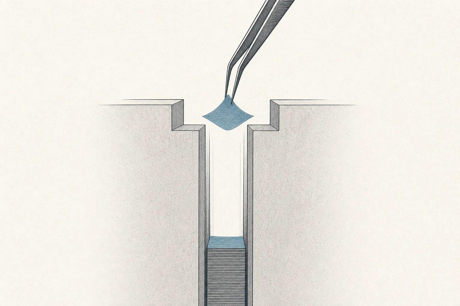
What makes these machines "hard" is that the newest chips are turning to vertical structures (like 3D NAND memory stacking over 200 layers, or gate-all-around transistors). The trenches to be etched get deeper and narrower — like having to drill a very deep well with a tiny mouth, and then coat its walls evenly from the top all the way down. That's exactly why ALD/ALE — adding and etching one atomic layer at a time — has become the hero of this era: it controls thickness with a precision the old methods can't reach.
04Where it sits in the chip world
If you see the whole chip factory as a production line, the deposition/etch machines are the central machines in the middle of the conveyor, where wafers run in and out over and over, on every layer. They work hand-in-hand with their neighbors on both sides, inseparably.
- Always paired with Lithography: litho "draws the pattern" with light onto the film deposition just coated; then etch carves along that pattern — the three steps alternate through the whole process. Without a film to print on, litho can't work
- Needs Metrology & Inspection to check: after each layer is added/etched, you need a machine to measure whether it's as thick as ordered, etched deep enough, and free of defects — because one bad layer can ruin the whole wafer
- Powers AI and Cloud & Digital Infrastructure directly: the AI chips and HBM memory that data centers fight over all pass through this group of machines first. The more AI grows, the better the machines sell — and it reaches on to Electrification & Mobility, Robotics, and Quantum Computing, which all need chips
- Depends on Critical Materials & Supply Chain: etching and coating use large amounts of special gases and high-purity chemicals, so this group of machines is sensitive to strains in the global raw-materials supply chain
05Where it stands now
The most shocking thing about this industry is its concentration — nearly all of the world's deposition, etch, and clean machines come from just three companies: Applied Materials, Lam Research, and Tokyo Electron together control about 70% of the market. Applied Materials is the strongest overall leader in coating (CVD/ALD), while Lam Research is the "king of etch," especially etch for 3D NAND memory and advanced logic.
The tailwind right now comes straight from AI. As the whole industry rushes to 3D chip structures — gate-all-around transistors and 3D NAND stacking hundreds of layers — the number of add and etch steps per chip jumps. In mid-2026, Applied Materials launched a new set of machines (the Centris ALD and Selectra etch families) designed specifically for the deep, narrow trenches of 3D chips — the more complex the chip, the more machines you need per wafer.
Another force shaking the board is the rise of Chinese players. Under pressure from U.S. export controls, China is racing to build its own equipment, and deposition/etch is where it's making the fastest progress — Chinese makers can now supply about 40% of the domestic market in etch and deposition tools, led by the "three musketeers" NAURA, AMEC, and ACM Research, which are already inside the real production lines of SMIC and YMTC.
06The road ahead — the atomic-scale era
The first direction is that everything goes vertical and atomic-scale. With shrinking chips horizontally nearly at the limits of physics, the way out is to build upward — gate-all-around, 3D DRAM, 3D NAND stacking more and more layers. Every layer added is one more add–etch cycle. This is the node's structural tailwind: demand grows not just with the number of chips, but with the "number of steps per chip" rising too.
The second direction is the split into two worlds. Export controls are pushing China to build its own tool supply chain in parallel with the West. In the short term this is a new chunk of demand (China rushing to buy/build tools at home), but in the long term it's a competitor slowly eating the three giants' share in the Chinese market — which used to be their largest.
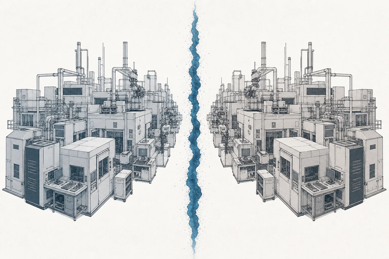
The third direction is that steps once overlooked gain value. Clean and selective deposition — once just supporting steps — become quality-deciders in complex 3D chips. That opens room for specialist players (in clean or ALD, say) to grow even without competing head-on with the overall leaders.
07Challenges & risks
The first risk is severe boom-and-bust cycles (cyclicality). Equipment sales are tied to chip factories' investment cycles, which rise and fall in big waves. When the chip industry booms, factories rush to order machines and revenue soars — but when the cycle turns down, orders can vanish for years. It's a high-margin business, but one you have to endure the swings of.
The second risk is the double-edged sword of geopolitics. Export controls cut off the chance to sell advanced machines to China, even though China was once the largest market for Western tool makers. Not being able to sell only speeds China up in building its own machines — and in the end, the three giants risk losing both today's sales and their long-term share in the Chinese market.
The third risk is concentration and dependence on a few customers. With the market controlled by three companies, and only a handful of end customers buying the most advanced machines (TSMC, Samsung, Intel, SK hynix, Micron), the big orders are concentrated in a few hands — if any one of them delays its investment plans, the tool makers' revenue shakes right away.
In short: this node is the construction crew that actually builds every single transistor, one layer at a time, adding then etching hundreds of times over. It's one of the most powerful bottlenecks in the digital economy — and the more complex chips get, the more important the role of the "adders and etchers" becomes.