Megatrend · Semiconductors
A chip is built a hundred layers at a time — and without someone to "check" every layer, the whole fab just makes expensive scrap
Lithography machines print the circuit pattern, and deposition/etch machines build transistors up one layer at a time. But there's another group of machines — the quietest and the most powerful. Their job is to "measure" whether every layer is the right thickness, and to "look" for tiny nano-scale defects that can kill a whole chip. This is Process Control. In a world where one chip costs a fortune, "good chips per wafer" (yield) is money — and the company that owns this market is a single name, KLA, with about 58% of the world.
01What it is
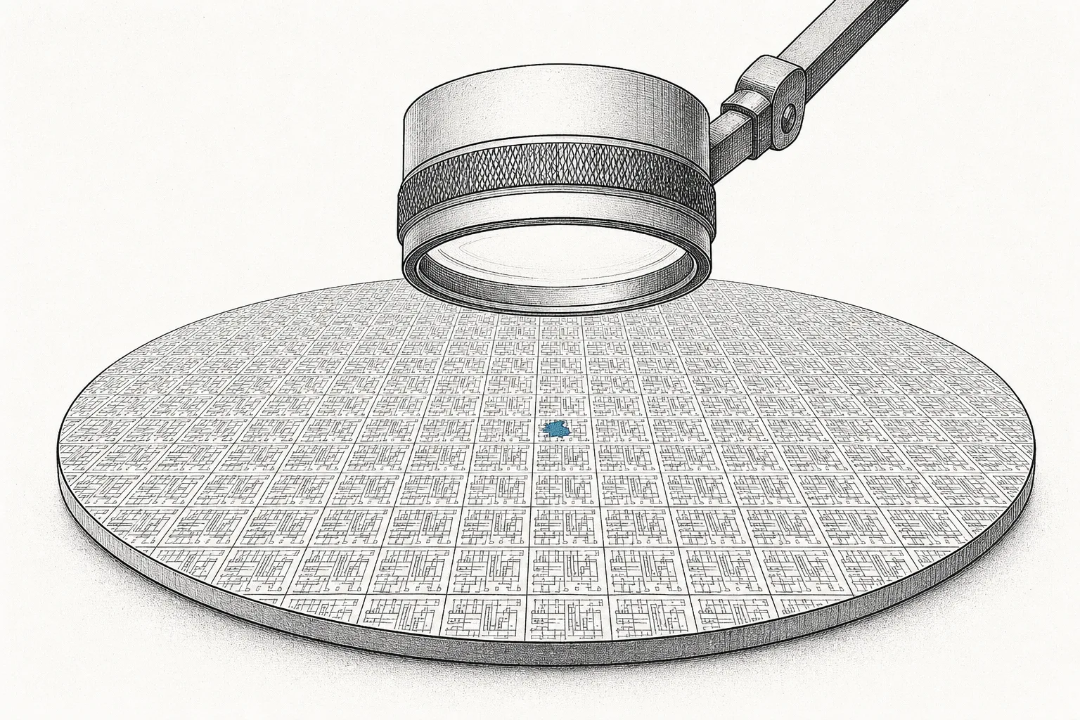
Picture building a 100-story skyscraper — but every floor is ten thousand times thinner than a human hair. And if floor 30 has just one tiny crack, the whole building is ruined. The question is: how do you know each floor was built "exactly" right before you stack the next one on top? The answer is this node: Process Control — the family of tools that "measure" and "look for defects" on every layer of a chip, before a mistake gets buried where you can't fix it.
Its work has two main legs. The first is Metrology (measurement) — checking whether the film you just deposited is as thick as specified, how fine the line pattern is (called critical dimension, or CD), and whether the top layer's pattern lines up exactly with the layer below or is shifted (called overlay). The second is Inspection (defect hunting) — sweeping across the whole wafer to find "foreign" things that shouldn't be there, like dust, scratches, or a missing pattern — both on the wafer itself and on the mask/reticle that prints the pattern.
On the megatrend map, this node is a sub-branch under Wafer-Fab Equipment & Lithography, inside the big trend Semiconductors. It sits in the "deepest layer of the supply chain" — it makes the tools that chip fabs then use. Its siblings next door are Lithography Systems (the pattern-printing machines ASML dominates) and Deposition, Etch & Process Tools (the machines that actually deposit and etch to build transistors) — if litho is the "draftsman" and dep/etch is the "construction crew," this node is the "construction inspector" (QC inspector), standing beside the line checking whether the other two groups' work is actually correct.
CD (Critical Dimension) = the width of the smallest line on a chip, which must be measured to nanometer accuracy · Overlay = the misalignment between the top layer's pattern and the layer below (they must stack exactly, or the wiring won't connect) · Defect = a flaw or foreign object on the wafer, from dust to a distorted pattern · Yield = the share of "good chips" out of all the chips on a wafer — the number that decides whether a fab makes money or loses it
02Why it matters — because yield is money
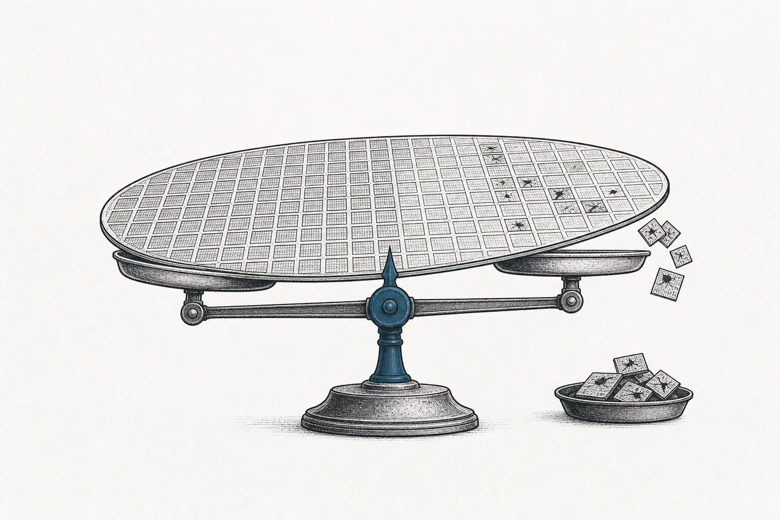
You can understand the chip business in one sentence: a fab has almost no cost "per chip" — only cost "per wafer". One advanced wafer goes through hundreds of process steps, takes months, and costs tens of thousands of dollars to make. Whether you end up with 90% good chips or 50%, the cost you paid is the same. So a fab's entire profit comes down to one number — yield, the share of good chips per wafer. And the machines that protect that yield are the ones in this group.
The math gets brutal here: a modern AI chip is huge, taking up a lot of wafer real estate, so a single wafer fits only a few dozen. One small defect landing in the wrong spot = one chip worth thousands of dollars dies on the spot. The bigger and pricier the chip, the more enormously it pays to catch a defect "first" — industry research estimates that better metrology can lift a fab's yield by about 2–3%. That sounds small, but on revenue in the tens of billions, it's hundreds of millions of dollars of profit a year.
The market reflects this clearly. The global Process Control machine market (metrology + inspection) was worth about $12 billion in 2025 — and more interesting than the figure itself is that it's growing faster than the overall chip-equipment market. Process control's share of total equipment spend (WFE) is climbing from about 7.4% in 2025 toward ~9% by 2030 — because the more complex chips get, the more often and more finely they have to be "checked."
03How it works (scan → measure/compare → flag defects)
The heart of a defect-hunting machine is a simple game that's massively hard to do: compare what "should be" against what "actually is". Because the patterns on a wafer repeat in millions of identical sets, the machine scans point by point, then compares this point to the neighboring point that should look exactly the same — wherever they "differ," that's a suspect defect. Let's walk through it step by step.
The "hard" part comes from two directions. The first is the defects keep getting smaller. In 2–3 nanometer chips, a chip-killing defect might be just a few nanometers across — smaller than the wavelength of ordinary light, so a normal optical camera can't see it. You have to turn to an electron beam (e-beam), which is finer but far slower. The second is volume — a single wafer has billions of patterns, and looking at every one fast enough to keep up with real production is a monstrous engineering problem. That's why these machines cost tens of millions of dollars each.
Optical inspection = uses light, very fast, can sweep an entire wafer quickly, good for finding defects big enough to see (it's the best-selling machine, and KLA holds over 85%) · E-beam inspection = uses an electron beam instead of light, far finer, sees nano-scale defects light can't — but slower; used when you need the ultimate resolution on advanced chips
04Where it sits in the chip world
If you see the whole fab as a production line, Process Control is the inspector standing at every point on the line. It builds nothing itself, but it's the one that decides whether every other machine's work "passes" or "fails" — which ties it inseparably to every neighbor.
- Inspects the work of Lithography: after litho prints a pattern, an overlay tool must immediately check how many nanometers the new layer is shifted over the old one. If it's out of spec, you can still strip and reprint before etching — but let it slip through and etch it, and the loss is permanent
- Inspects the work of Deposition & Etch: every time you deposit a film or etch a trench, a tool has to measure whether the thickness/depth is exact and no foreign matter is left — because dep/etch repeats hundreds of times, and one missed round gets buried where you can't fix it
- A direct quality gate for AI and Cloud & Digital Infrastructure: the big AI chips and HBM that data centers fight to buy already have lower yield than ordinary chips (because they're large and complex), which makes good inspection the thing that decides whether you can make enough to sell — this node is the gatekeeper of yield in the AI era
- Underpins Electrification & Mobility, Robotics and Quantum Computing: every industry that needs reliable chips (especially automotive chips, where failure is not an option) leans on quality inspection at this level
05Where it stands now
The strangest thing about this node is that it's owned, completely, by a single company — KLA Corporation holds about 58% of the world's process control market (up from about 54% in 2021 to 2026), and in the best-selling optical inspection machines KLA holds over 85%. KLA is number one in 7 of the 10 process control sub-segments — a level of dominance that's rare even in an already highly concentrated chip industry. In fiscal 2025 KLA posted revenue of about $12.2 billion and net profit of $4.06 billion — margins that show just how much the "sharpest eyes" can sell for.
But KLA's dominance doesn't mean no one else survives, because process control has many deep specialist corners where a "small player" holds equally complete control. The best example is Japan's Lasertec — the only company in the world that makes "blank mask" inspection machines for EUV at the true wavelength (actinic), priced at over $75 million each. In fiscal 2025 it booked ¥251.5 billion in sales (+17.8%) with an operating margin near 50% — a picture of how, in this field, "a small but indispensable niche" = lovely profits.
The tailwind right now comes straight from AI. Gate-all-around-era chips and ever-more-complex HBM need more frequent, finer inspection, so KLA is rushing out new e-beam and optical machines (like Gen 4) designed specifically for the new transistor structures. Process control's share of total equipment spend is gradually climbing for this reason — the harder chips get, the more the world has to invest in "inspection."
06The road ahead
The first direction is that "inspect more" becomes the iron law of new-generation chips. As chips move to vertical structures (3D NAND stacked hundreds of layers high, gate-all-around, 3D DRAM), defects hidden under deep layers get harder to find, and the cost of "missing it without knowing" gets higher. The result: the number of measurement/inspection steps per chip keeps rising — this is the structural tailwind that makes this market grow faster than the industry average, pushing process control's share of WFE from ~7.4% in 2025 toward ~9% in 2030.
The second direction is AI coming in to help "read defects". Inspection machines generate an enormous number of images per wafer. The new challenge isn't just to "see" a defect, but to "tell apart" which kind of defect truly kills a chip and which is harmless — especially when ramping a new production node that has no defect data to learn from yet. So machine learning has become the new arena: whoever classifies defects more accurately and faster helps customers climb yield faster.
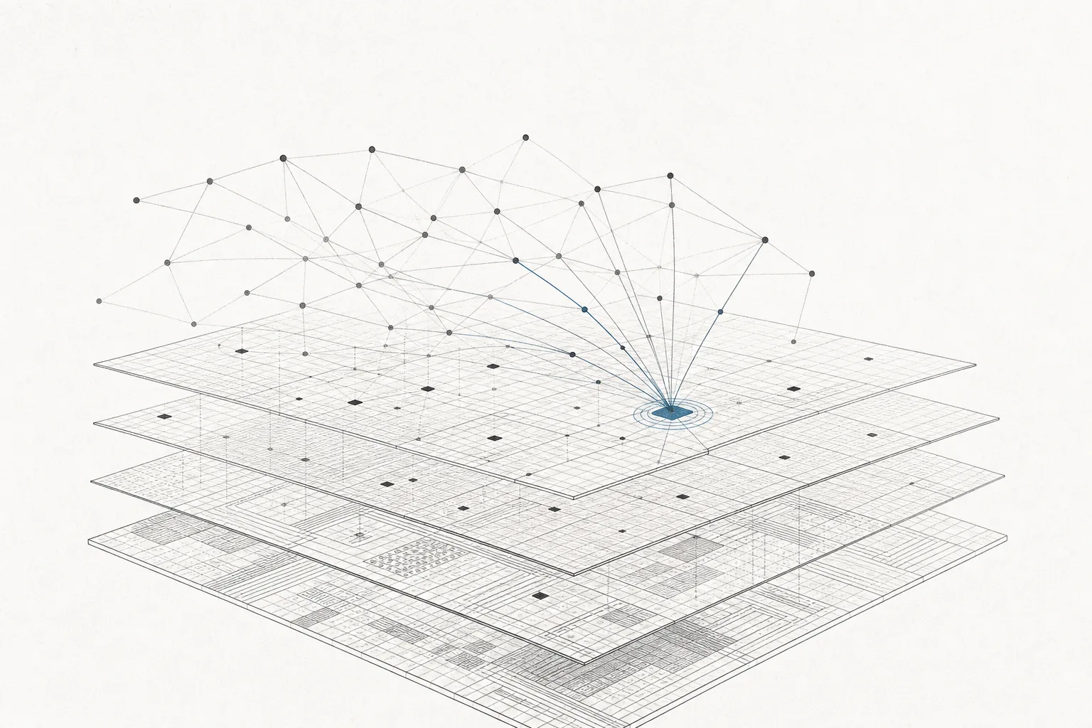
The third direction is inspection in advanced packaging. As new-generation chips are no longer made as a single piece but by joining several smaller chips together (chiplet, hybrid bonding), the junctions between pieces become a whole new gate that needs inspecting — opening room for specialist players like Camtek and Onto Innovation, strong in packaging inspection, to grow even though they don't compete head-on with KLA in the main market.
07Challenges & risks
The first risk is extreme concentration. A market where one company takes more than half is a double-edged sword — it's a beautiful moat for the market leader, but it also means the world's entire chip industry depends on the decisions, quality, and continuity of a handful of players. If they stumble (technology can't keep up, supply problems), the impact spreads across the whole industry.
The second risk is severe boom-and-bust (cyclicality). Equipment sales are tied to chip fabs' investment cycles, which swing up and down in big waves. When the industry booms, fabs rush to order machines and revenue surges — but when the cycle turns down, orders can vanish for years. It's a high-margin business that has to endure volatility, and because process control is expensive equipment, fabs tend to be among the first to hold off buying when they tighten their belts.
The third risk is geopolitics and China. China used to be KLA's biggest market — China's share of KLA's revenue fell from 41% in 2024 to ~30% in 2025 as US export controls tightened. This is a double-edged sword: on one side it cuts off a large chunk of sales on the spot, on the other it speeds up China's push to build its own machines. Chinese players like Skyverse (added to the Entity List in December 2024) are chasing domestic inspection machines — even though metrology/inspection is one of the spots where China is still "weakest" compared with etch/deposition.
In short: this node is the inspector standing at every point on the line, measuring and hunting for defects on every layer of a chip, before a mistake gets buried and ruins the whole wafer. It's one of the quietest yet most powerful bottlenecks in the digital economy — because in a world where one chip keeps getting more expensive, "seeing the defect first" is what separates a profitable fab from one that makes expensive scrap.