Megatrend · Semiconductors
One machine, $380 million, 165 tons — and it decides whether the world ever gets faster chips
Before any AI chip can exist, it has to be 'printed' with light — projecting a circuit pattern through a mask onto a silicon wafer, with lines tens of thousands of times finer than a human hair. The machine that does this is the most expensive and most complex tool in a chip factory, and only one company on Earth can build the top-end version — ASML of the Netherlands, which owns 100% of EUV. This is the story of the real bottleneck that decides whether Moore's Law keeps moving.
01What it is
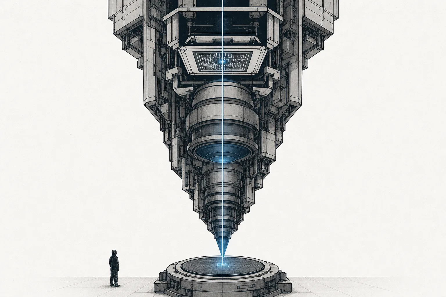
Think of developing photos the old way — you shine light through a film carrying an image onto light-sensitive paper, and the image appears. Lithography is exactly the same printing, except the 'image' is a chip's circuit pattern and the 'paper' is a round silicon disc coated with a light-sensitive material. The lithography machine shines light through a mask carrying the circuit pattern, then shrinks that image many times over so it lands on the wafer — this is the 'printing' step that decides how small a chip's transistors can get.
Here's the heart of this node: the family of machines that use light to draw the pattern onto a chip. And how fine those lines can be depends on the wavelength of light used — the shorter the wave, the smaller the line. So the world has worked its way from longer light to shorter: DUV (Deep Ultraviolet, 193 nanometers) for ordinary and older chips · EUV (Extreme Ultraviolet, 13.5 nanometers) for the most advanced chips · and most recently High-NA EUV, which uses a bigger lens to draw even smaller.
On the megatrend map, this node is a sub-branch under Wafer-Fab Equipment & Lithography within the big trend Semiconductors. It's the 'pattern drawer' of the chip factory. Its siblings next door are Deposition, Etch & Process Tools (the construction crew that adds and carves material along the pattern litho drew) and Process Control — Metrology & Inspection (the inspection crew that checks the pattern is sharp and on-spec) — these three steps take turns hundreds of times to make a single chip.
DUV = deep-ultraviolet light at 193 nanometers, used for most of the world's chips (about 67% of the machine market) · EUV = extreme-ultraviolet light at 13.5 nanometers, 14x shorter, used to make the finest chips · NA = a number for the 'size of the lens' — the higher the NA, the more angles of light the lens captures, drawing lines sharper and smaller. High-NA (NA 0.55) draws down to 8 nanometers in a single exposure, versus ~13 nanometers for regular EUV in one shot.
02Why it matters — the bottleneck of Moore's Law
One law has driven the chip industry for almost 60 years, called Moore's Law — roughly every two years we can pack twice as many transistors onto a chip, making computers faster and cheaper. But this law only keeps going as long as we can actually 'draw the pattern' smaller, and what decides how small the lines can go is the lithography machine itself. Put simply — if litho doesn't move, the whole industry can't move.
Its market isn't the biggest among chip tools, but it's the point everything has to pass through. The lithography machine market in 2025 is worth about $28 billion and is expected to grow to about $41 billion in 2030 (~7% a year). But the number that really grabs you is the price per machine — one EUV machine runs ~$183 million, and the latest High-NA hits $380 million per machine, more than an entire passenger jet.
Most important of all is the concentration of power. Every EUV machine in the world — every single one — comes from one company: ASML of the Netherlands. ASML's share of the overall lithography market is about 94%, and in EUV it's a full 100%. There's no number two. That makes the lithography machine a 'strategic bottleneck' the US, China and the whole world watch closely — whoever controls this machine controls who gets to make advanced chips.
03How it works (light → mask → pattern)
The basic flow is like developing photos, but in the details it's unbelievable engineering. Let's walk step by step through how the circuit pattern travels from light to the silicon wafer.
The real difficulty is that EUV light is 'enormously hard to create'. The 13.5-nanometer light doesn't come from a bulb; it has to be made through a process that sounds like science fiction: tiny droplets of tin are fired into a vacuum chamber, 50,000 droplets a minute, and a high-power laser hits each one to turn it into superhot plasma. That plasma emits EUV light. Then special mirrors (not glass lenses, because EUV can't pass through glass) reflect the light to the mask and wafer. All of it has to happen in a vacuum, because even air absorbs EUV light completely.
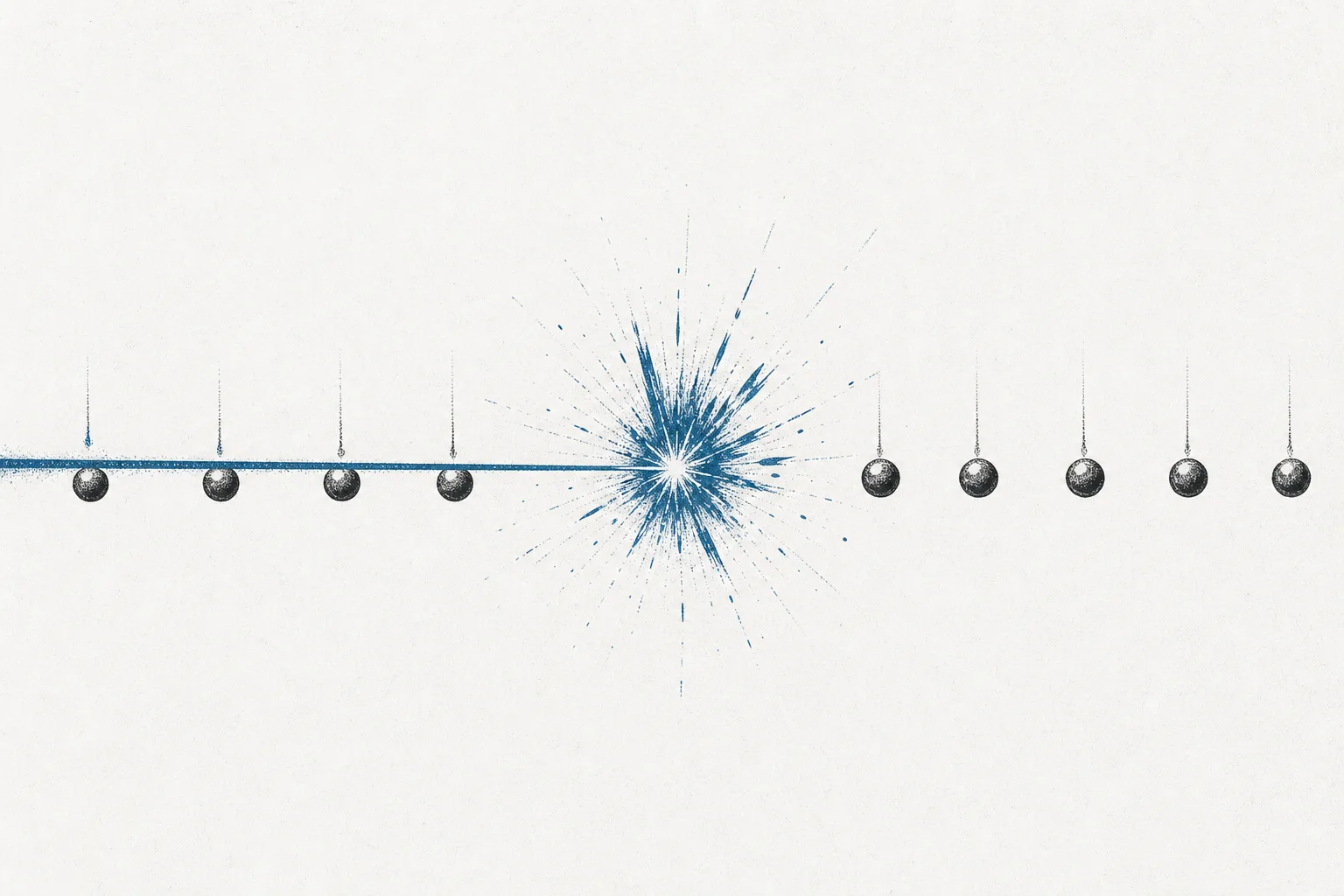
The 13.5-nanometer EUV light is so powerful that nearly every material absorbs it — even ordinary glass lenses and air. That makes camera-style lenses impossible for EUV; instead it uses multilayer specially coated mirrors (made by Germany's Zeiss), reflecting the light in sequence inside a vacuum. They have to be so smooth that if you scaled a mirror up to the size of a country, the roughness wouldn't exceed the height of a human hair — this is why only one company in the world can make this machine.
04Where it sits in the chip world
If you see a chip factory as a production line, litho is the pattern drawer that opens the work on each layer, then hands it off for the other machines to follow the design. It doesn't work alone — it coordinates inseparably with its neighbors.
- Always paired with Deposition & Etch: litho draws the pattern onto the light-sensitive material, but that pattern is still just a 'draft' — etch has to carve the material along the pattern, and deposition coats the next layer of film. These three steps cycle hundreds of times; if litho doesn't draw sharply, every step after it breaks too
- Needs Metrology & Inspection to check: after each print, you have to measure that the pattern is in the right place, the lines are sharp enough, and it overlays the previous layer to nanometer precision — because a print that's off by even a hair ruins the entire wafer
- A bottleneck that directly unlocks AI: AI chips like the GPUs and HBM memory data centers fight to buy all need EUV to print their patterns — so the exploding AI demand translates straight into orders for EUV machines. It carries on to Cloud & Digital Infrastructure, Electrification & Mobility, Robotics and Quantum Computing
- Leans on Critical Materials & Supply Chain: each machine is assembled from hundreds of thousands of parts from suppliers worldwide — Germany's Zeiss mirrors, TRUMPF lasers, masks and light-sensitive material — making it fragile to any strain in the chain
05Where it stands now
The standout story in this industry is ASML's almost unrivaled edge. In 2025 ASML posted total sales of €32.7 billion; EUV machine sales in particular grew 39% to €11.6 billion on 48 machines delivered, with a gross margin as high as ~53% — numbers that reflect the simple fact that when you're the only one in the market, you set the price.
The big milestone of this cycle is the arrival of High-NA. The first High-NA EUV machine (EXE:5200B) was delivered to Intel in Q4 2025, and Samsung ordered two for a combined ~$773 million, while TSMC announced it will use High-NA starting at the A14 node in 2028 — a machine that draws down to 8 nanometers in a single exposure, shrinking transistors about 1.7x and packing nearly three times the density.
So what about the other two? Japan's Canon and Nikon were market leaders 20 years ago, but both have pulled out of the EUV fight — Nikon is focusing on DUV machines and aims to launch a new ArF machine to catch up by 2028, while Canon chose a different path called nanoimprint (NIL) — instead of shining light, it 'stamps the pattern' by pressing a mold directly onto the wafer (its FPA-1200NZ2C machine reaches ~15 nanometers). It's cheaper and uses less power, but hasn't yet proven itself in high-volume production.
The other thing shaking up the board is China's catch-up. Under export controls that block EUV and advanced DUV machines, China is racing to build its own, led by SMEE, which can already make 28-nanometer-class DUV immersion machines — but still has to rely on Zeiss mirrors and Cymer light sources from abroad, and use multi-patterning to compensate. The gap with ASML is still years wide, but the direction is clear.
06The road ahead — High-NA and beyond
The first direction is High-NA becoming the new standard for advanced chips. ASML is targeting 20 High-NA machines a year by 2028 and already has orders for '10–20 machines' from Intel, SK hynix and Samsung. As chips keep shrinking, a single High-NA exposure replaces the multiple exposures of regular EUV — fewer steps, more precision, but at double the price.
The second direction is the chase for ever-shorter wavelengths. After High-NA (NA 0.55), ASML's roadmap extends to Hyper-NA (an even higher NA) to stretch Moore's Law out another decade. But each step gets exponentially harder and more expensive — bigger lenses, more complex machines, and new light-sensitive materials and masks the whole chain has to develop in step.
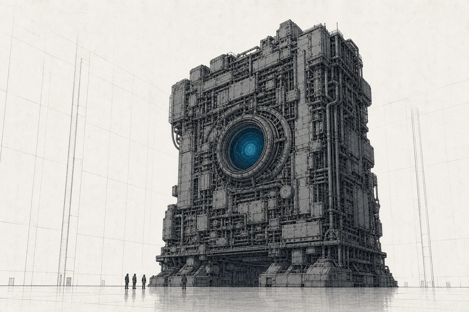
The third direction is the split into two worlds. While the West chases High-NA and Hyper-NA, China is forced to build its own path in parallel — racing to develop domestic DUV and searching for a 'shortcut' to its own EUV. In the short term this is a new chunk of demand as China rushes to buy and build machines, but in the long term it means a single market fracturing into two technology systems that develop separately.
07Challenges & risks
The first risk is single-vendor concentration. The fact that every EUV machine in the world comes from ASML alone is both the company's strength and the whole industry's fragility — if ASML's production line stalls, whether from disaster, a supplier problem, or an incident at a single factory, the entire world can't make advanced chips. There's no backup plan, because there's no number two.
The second risk is export controls and geopolitics. The lithography machine has become a weapon in the tech war. The US has pressured the Netherlands to bar selling EUV and advanced DUV to China, even though China was once a big market for ASML — so revenue from China is at risk of being cut off, and the more pressure is applied, the faster China builds its own machines. In the end it could lose both today's sales and its long-term share.
The third risk is cyclicality and dependence on a handful of customers. The most advanced EUV machines have only a few real customers — TSMC, Samsung, Intel, SK hynix. If any one of them delays its investment plans or slows a new node, an enormous chunk of orders vanishes at once. And because each machine costs hundreds of millions, the decision to buy is very sensitive to the economic cycle and confidence in chip demand ahead.
In short: this node is the machine that prints the pattern of every chip with light — it decides how small a transistor can get, and with it, whether Moore's Law keeps moving. It's the narrowest, most expensive and most concentrated bottleneck in the digital economy — whoever controls this machine controls the future of the world's computing power.