Megatrend · Critical Materials
The stuff that's less than 1% of a chip's cost — but if it runs out, the whole fab stops
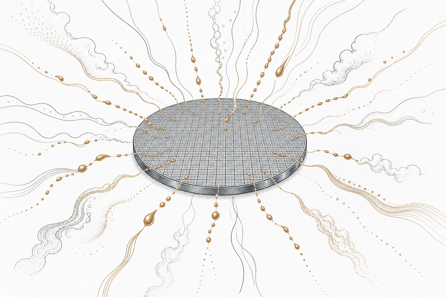
The world talks about TSMC, NVIDIA, and multi-billion-dollar EUV machines. But no chip can exist without another pile of "snacks" almost nobody sees — photoresist, polishing slurry, specialty gases, and metal sheets purified to nine-nines — fed onto the wafer drop by drop across hundreds of steps. Together they're a market of just ~$67 billion — a fraction of the chip value they create — yet some have only 2–3 makers on Earth, and almost all of them are in Japan. This is the truest chokepoint of the chip era.
01What it is (the invisible consumables)
When we talk about "making chips," we usually picture giant billion-dollar machines like ASML's EUV tools and TSMC's fabs. But inside a fab, a single silicon wafer doesn't just get "blasted with light" — it has to be coated, deposited, etched, polished, and washed with dozens of ultra-high-purity chemicals and materials, over and over, hundreds of times, before it becomes a single chip.
That's the heart of this lesson — electronic & semiconductor materials, the consumables used up in making chips, displays, and printed circuit boards (PCBs). Not the machines, not the chips, but the "food" fabs have to refill every day. There are five main families:
Photoresist = a light-sensitive liquid spread thin on the wafer to "receive" the circuit pattern from light · Wet chemicals / CMP slurry = acids, solvents, and tiny polishing powders used to etch and "shave the wafer's surface flat to the atom" · Specialty / electronic gases = ultra-high-purity gases used to etch, deposit, and dope the silicon · Sputtering targets = pure metal sheets (copper, tantalum, tungsten) "shot" so their atoms fly off and deposit as a thin film on the wafer · Precursors = starter molecules that vaporize and build nanometer-thin films one layer at a time.
The key is to tell it apart from its "close relatives." On our megatrend map, this node is a sub-branch of Specialty Chemicals & Industrial Gases under Critical Materials & Supply Chain — it's the "consumables that get used up," while the starting wafer and base substrate live in another node, Semiconductor Materials. Put simply: that node is the "blank paper," and this node is the "ink and chemicals" that draw the circuit onto it.
02Why cheap stuff is a chokepoint for the whole industry
Start with size. The global semiconductor-materials market is around $67.5 billion in 2024 and hit a new record of $73.2 billion in 2025, per SEMI. That sounds like a lot, but it's a fraction of the chip value it creates — the global chip market is over $600 billion, and those chips drive a digital economy worth trillions.
This block of materials splits into two big buckets. The first is wafer fab materials, around $42.9 billion — the photoresists, chemicals, and gases used while building the circuit on the wafer. The other is packaging materials, around $24.6 billion, used when the chips get packaged into individual units.
Now the heart of it: why does "cheap stuff" have such enormous power? The answer is cost. Look at this number: a single 300mm wafer built on the most advanced technology (say, 3 nanometers) can be worth up to ~$25,000, yet all the chemicals and materials used on that wafer add up to only about $2,000 — less than a tenth of its value.
But cheap doesn't mean unimportant — quite the opposite. Some of these have only 2–3 makers on Earth, and switching one chemical's formula takes a year of testing and qualifying on the production line. If the main photoresist runs short, a $200 million EUV machine just sits there idle, because there's nothing for it to "expose." That's what chokepoint means — cheap stuff that, if it runs out, stops the whole line.
03How it works (feeding materials onto the wafer, drop by drop)
The easiest way to understand this node is to see chipmaking as a "chemical assembly line." A blank wafer goes in and loops through the same stations hundreds of times, with different material families "fed in" at different moments each cycle. Let's trace where each material comes in.
The real difficulty of this business isn't "making the chemical" — it's how "clean" you can make it. In the world of chips, impurities down to "a few atoms per billion" can ruin a whole wafer. The starting silicon has to be pure to 99.9999999% (what the industry calls "9N," or nine-nines), and the gases and chemicals have to be just as pure. This is the node's moat — whoever makes their stuff the cleanest and most consistent wins.
04What it connects to
This node sits "upstream" of the entire digital world. Its inputs come from Industrial Gases (a sibling under the same parent node, feeding basic high-purity gases) and Semiconductor Materials (the wafers and base materials this node "draws circuits" onto) — two close relatives that work side by side in the same fab.
But what matters more are the "mouths waiting to be fed" downstream. These materials feed straight into Semiconductors — the heart of every chip — and those chips flow on to feed almost every megatrend of the era: Artificial Intelligence and Cloud & Digital Infrastructure (modern AI chips are more complex and eat more steps and chemicals), Electrification & Mobility (power chips in EVs), and Defense & Geopolitical Fragmentation (military and space chips).
05Where it stands now
There's one thing you have to grasp about this field first: how concentrated it is in a few countries, especially Japan. The clearest example is photoresist — Japanese companies control about 75% of the world's semiconductor-photoresist market, and if you narrow it to resist for EUV (the leading-edge technology), three Japanese firms — Tokyo Ohka Kogyo, JSR, and Shin-Etsu — together hold over 90%.
Why does this matter? Because the world has already seen this chokepoint used as a "weapon." In July 2019, Japan announced controls on exports of three chip chemicals to South Korea — advanced photoresist, hydrogen fluoride (HF), and fluorinated polyimide — requiring a license for each shipment. Korea was shaken instantly, because Samsung and SK Hynix together make 72% of the world's DRAM and half its NAND flash. HF exports from Japan to Korea dropped 87.9% during that stretch.
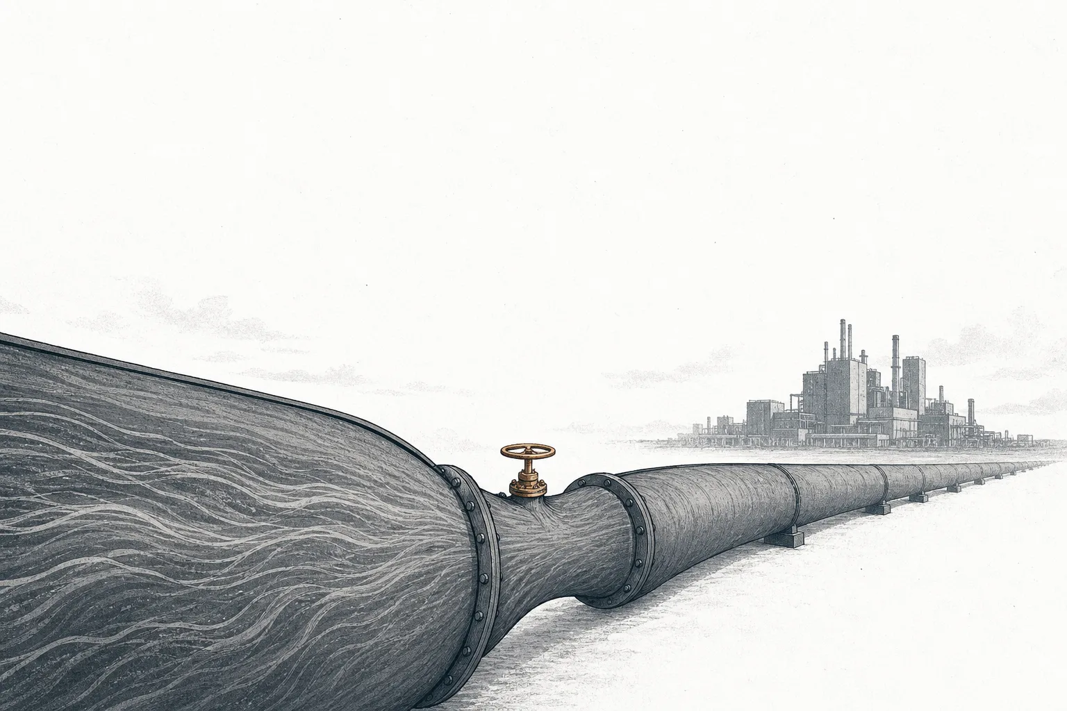
Korea hit back by racing to find "non-Japan" sources and build supply at home — SK Hynix poured about ₩320 billion ($268 million) into qualifying domestic materials between 2019 and 2021, and by 2022 the share of fluorinated polyimide Korea made itself rose from 3.1% to 18%. This episode became a wake-up call for the whole world to start seriously "diversifying" its chip-materials supply chain.
Another field just as hot is CMP slurry — a market of about $1.78 billion in 2024 where players like Japan's Resonac, DuPont, Merck (Versum), and Cabot compete fiercely. The more circuit layers a chip stacks (some over 100), the more often it needs polishing flat, so slurry is one of the fastest-growing groups. In this field, the real players split into three camps: Japanese materials giants that control photoresist and slurry, Western chemical/materials firms that sell purity and delivery systems, and Asian challengers climbing up in specialty materials.
06The road ahead
Three forces will shape this business. One — the High-NA EUV era needs a new set of chemistry. Finer and finer chips need new photoresist formulas that are faster and sharper. The EUV-specific photoresist market alone is jumping from ~$226 million in 2024 to about ~$879 million by 2030 (over 25% a year) — several times faster than the overall materials market — and it's a field where the three Japanese firms still lead by a wide margin.
Two — every country wants its own materials supply. The 2019 lesson pushed the US, Europe, Korea, and China to pour money into building chip-materials plants at home, so no one can "shut the tap" on them again. This spreading of production opens doors for new players, but it also means more competition and more duplicated investment.
Three — advanced packaging materials are becoming a new field. As shrinking transistors starts hitting the limits of physics, the industry is turning to "stitching several chips together" (advanced packaging / chiplets) instead, which needs lots of new packaging materials — which is why the packaging-materials pile ($24.6 billion) is becoming a growth engine that giants like Resonac and Kingboard are betting heavily on.
07Challenges & risks
Concentration is double-edged. Having only 2–3 makers of some critical items gives the leaders pricing power and fat margins, but it also makes the whole industry fragile. A single natural disaster, a fire at one plant, or one geopolitical clash can cut off world supply overnight. And most recently, in 2025, there were rumors Japan might restrict photoresist exports to China, which instantly worried China's chip industry.
The same moat that protects you can lock you out. Because customers need a year to qualify a new material, incumbents gain a huge edge — but it also means new challengers (especially from China and Korea) break in slowly and with great difficulty, even if their product is nearly as good. So competition moves slowly and is decided by "trust" more than price.
You can't avoid following the chip cycle. Even as the fab's "daily food," material volumes are tied directly to the chip industry's ups and downs. When chip demand softens (like during a memory glut), fabs cut output and material sales shrink with them. So this node reaps the full upside of the AI wave — but also takes the full hit when the cycle flips.